
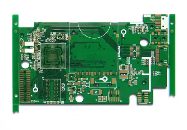
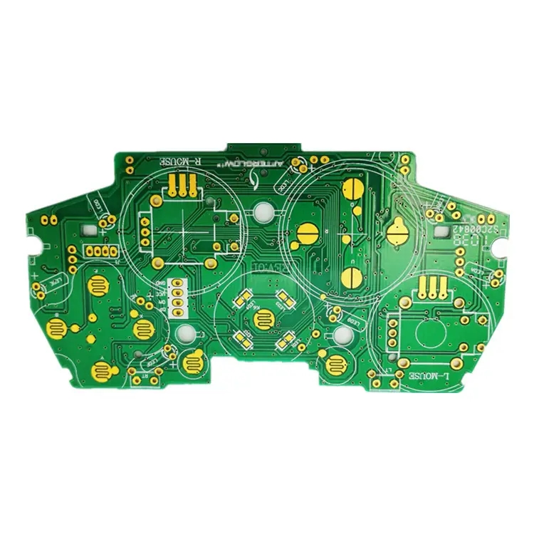
Professional PCB manufacturing and assembly
Building 6, Zone 3, Yuekang Road,Bao'an District, Shenzhen, China
+86-13410863085Mon.-Sat.08:00-20:00

Explain in detail the use of circuit board surface mount technology CSP and passive components
CSP usage
Nowadays, a common key skill is CSP. The charm of CSP skill lies in its many advantages, such as reducing the package size, adding the number of stitches, function/function enhancement, and the reworkability of the package. The efficient advantages of CSP today: when it is used for board level assembly, it can cross the boundary of peripheral package with a small distance (as thin as 0.075mm) and enter the array layout with a large distance (1, 0.8, 0.75, 0.5, 0.4mm).
Many CSP devices have been used in the field of consumer telecommunications for many years, and they are widely considered as low-cost solutions in the fields of SRAM and DRAM, medium pin number ASICs, flash memories and microprocessors. CSP can have four basic characteristics: rigid base, flexible base, lead structure base and chip level planning. CSP skills can replace SOIC and QFP equipment and become mainstream component skills.
One of the difficulties in CSP assembly process is that the bonding disk for welding interconnection is very small. Generally, the bonding disk size of 0.5mm away from CSP is 0.250-0.275mm. With such a small scale, it is difficult to print solder paste through openings with an area ratio of 0.6 or even lower. However, printing can be carried out successfully by using carefully described techniques. The onset of the problem is usually due to the lack of solder caused by blocking the opening of the template. The board level reliability mainly depends on the package type, while the CSP equipment can experience an average thermal cycle of 800~1200 times at - 40~125 ℃, and can be filled without down filling. However, if you select the lower fill data, most CSPs add 300% of the thermal stability function. CSP equipment defects are usually related to solder fatigue and cracking.
Forward of passive components
Another new category is 0201 passive component skills. Because of the market need to reduce board size, people attach great importance to 0201 components. Since the introduction of 0201 components in the middle of 1999, cellular phone manufacturers have assembled them together with CSP into the phone, which has reduced the size of printed boards by at least half. Proper handling of such packages is troublesome. To reduce the presentation of post process defects (such as bridging and upright), the key is to optimize the pad size and component distance. As long as the description is reasonable, these packages can be placed close to each other, and the distance can be as small as 150 mm.
In addition, 0201 equipment can be placed under BGA and larger CSP. Cross sectional view of 0201 below 14mm CSP assembly with 0.8mm distance. Because the scale of these small discrete components is very small, the assembly equipment manufacturer has developed an updated system that is compatible with 0201.
By 2009, the actual mass production of mobile phones has adopted the manufacturing process of 01005 (English system, metric system is 0402). By 2013, 03015 (metric system) and below parts have entered the stage of mounting experiment.
Through hole assembly still has vitality
Optoelectronic packaging is widely used in telecommunications and networks where high-speed data transmission is prevalent. Generally, board level optoelectronic equipment is a "butterfly" module. Typical leads of these devices extend horizontally from the four sides of the package. The assembly method is the same as that of through-hole element equipment. Usually, the technical process is used - the lead is processed by the lead forming pressure and pierced into the access hole of the printed plate to penetrate the substrate.
The first difficult problem to deal with this kind of equipment is that the lead can be damaged at the time of lead forming process. Because such packages are very valuable, it is necessary to be careful to handle them to prevent the lead from being damaged by molding operation or the module package at the lead equipment body title interface from cracking. In the final analysis, the best solution to combine optoelectronic element equipment with standardized SMT products is to select active equipment. In this way, the element equipment is taken out of the disk, placed on the lead molding thing, and then the equipment with lead is taken out of the molding machine, and finally the module is placed on the PCB. In view of the fact that this kind of selection needs to be funded by equipment with appropriate large cost, most companies will continue to select craft assembly process.
Large scale printing plate (20 × 24 ″) is also widely used in many production areas. For example, products such as set-top boxes and routing/switching printed boards are quite messy, including a mixture of various skills reviewed in this article. For example, large ceramic gate arrays (CCGA) and BGA devices as large as 40mm2 can often be seen on such PCBs.
The two primary problems with this type of equipment are large heat dissipation and heat induced warping effects. These elements can play the role of a large heat sink, resulting in uneven heating under the package surface. Because the thermal control and heating curve control of the furnace can make the middle of the equipment adjacent to the non humid welding connection. Warpage of equipment and printed boards caused by heat at the time of disposal will cause "non moisture appearance" such as separation of components from solder paste applied to PCB. Therefore, it is necessary to be careful when mapping the heating curve of these printing plates to ensure that the BGA/CCGA surface and the entire printing plate surface are evenly heated.
The circuit board manufacturer, circuit board designer and PCBA processor will explain the use of CSP and passive components in detail.


Just upload Gerber files, BOM files and design files, and the KINGFORD team will provide a complete quotation within 24h.