
Professional PCB manufacturing and assembly
Building 6, Zone 3, Yuekang Road,Bao'an District, Shenzhen, China
+86-13410863085Mon.-Sat.08:00-20:00


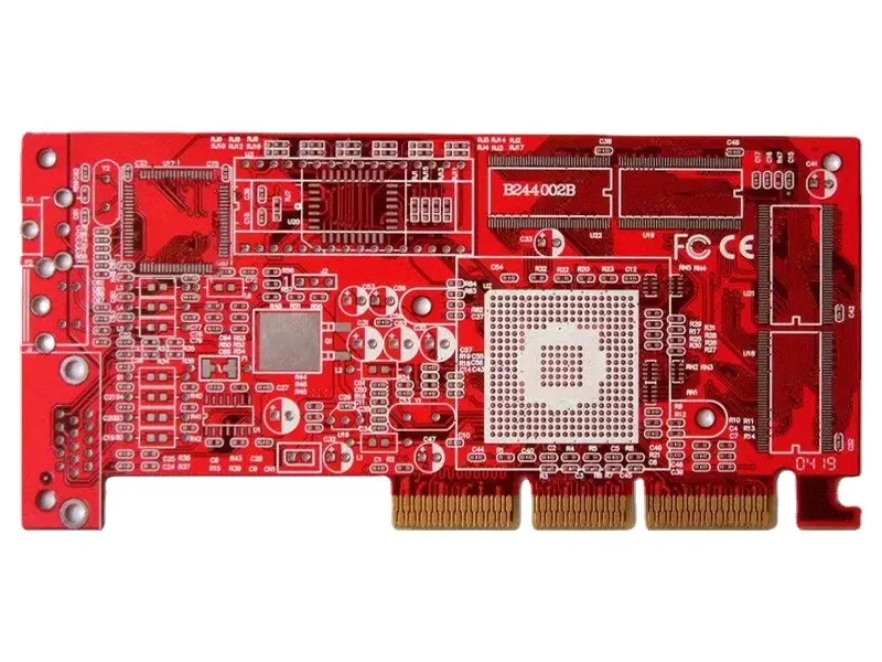
How to do a good job of electrostatic protection in PCBA processing
In the process of PCBA processing, electrostatic protection is very important. Static electricity will damage electronic components invisibly, thus affecting the quality of products. In the eyes of PCBA manufacturers, the quality of products depends largely on the electrostatic protection at the production site. Next, it is necessary to do a good job in electrostatic protection for PCBA processing, as well as precautions and work points for doing a good job in electrostatic protection. Why does PCBA processing need static electricity protection? There are many precision electronic components on the PCBA board, many of which are sensitive to voltage. Impulse higher than rated voltage will damage these components. The PCBA board damaged by static electricity is difficult to be checked step by step during the function test. What is more fatal is that some PCBA boards function normally during the test, but when the finished products are used in the hands of customers, they have occasional defects, which bring great hidden trouble to after-sales service and affect the company's brand and goodwill. Therefore, ESD electrostatic protection must be highly valued during PCBA processing.
Electrostatic hazards faced by PCBA processing
According to the timeliness, we divide the damage into two types, one is sudden damage. This kind of damage can usually be found in the quality inspection during the production process. Usually, the only loss brought to the enterprise is the cost of rework and repair. 2. Potential damage generally refers to that the basic use function of the components still exists, but the service life decreases sharply. Usually, it can only be found when it is used by later users. This kind of damage will cause many unexpected losses.

Precautions for electrostatic protection during PCBA processing
1. The operator must wear static work clothes. It is forbidden to attach or wear any metal products on the work clothes. It is not allowed to take off the work clothes at the site where static sensitive products are operated. All buttons of the work clothes must be buttoned up to prevent them from being undressed as far as possible. 2. Wear an anti-static wrist, with the wrist strap in good contact with the skin and reliably grounded. It is not allowed to stack plastic boxes, rubber, cardboard, glass and other sundries that are easy to generate static electricity on the electrostatic safety workbench. 3. All components must be operated on the electrostatic safety workbench. All components entering the anti-static work area must be treated according to anti-static requirements. 4. Electrostatic sensitive elements falling on the floor during operation must be tested and reconfirmed before use. Articles that cannot be tested directly can only be released after being confirmed as qualified. 5. When holding the sensitive element, avoid contacting its leads and lugs. Keep the motherboard away from the area of electrostatic sensitive components. When some components need to be cleaned, anti-static brush should be used instead of plastic brush. 6. When entering the workshop, you must wear an anti-static cap to prevent your hair from inadvertently contacting with static sensitive components. 7. During manual welding, anti-static low voltage constant temperature electric soldering iron shall be used, and it is prohibited to repeatedly use device packaging tubes to package components.
Key points of electrostatic protection in PCBA processing
1. Ensure that the temperature and humidity of the workshop are within the standard range, 22-28 ℃, and the humidity is 40% - 70%; 2. All employees must discharge static electricity when entering or leaving the workshop; 3. Dress as required, wear static cap, static clothes and static shoes; 4. All stations that need to touch the PCBA board must wear a corded electrostatic ring and connect the corded electrostatic ring to the electrostatic alarm; 5. The static wire is separated from the ground wire of the equipment to prevent the equipment from leaking electricity and causing damage to the PCBA board; 6. All electrostatic frame racks of turnover vehicles must be connected to the electrostatic ground wire; 7. ESD static spot inspection shall be carried out in strict accordance with ISO quality management requirements. Static electricity can not be seen or touched in the production process. It often inadvertently causes fatal hazards to PCBA circuit boards. The cost of PCBA troubleshooting is very high. Therefore, the managers of each factory must attach great importance to ESD static electricity management, so that the PCBA processing process can be completely controlled.
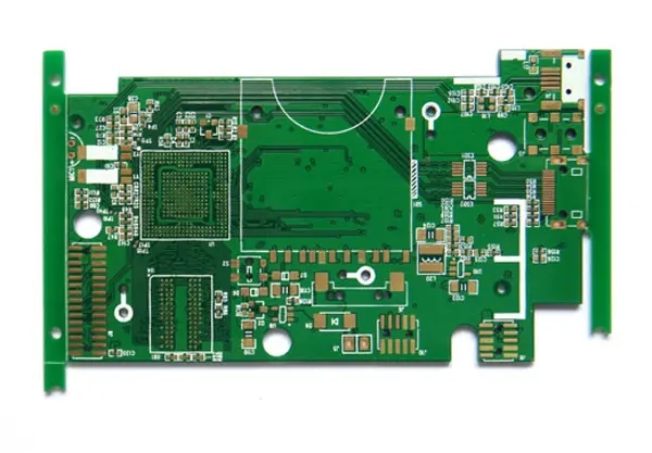
How to do solder paste printing well in PCBA processing
PCB company specializes in providing overall PCBA electronic manufacturing services, including one-stop services from upstream electronic component procurement to PCB production and processing, SMT patch, DIP plug-in, PCBA testing, and finished product assembly. Next, we will introduce how to do solder paste printing well in PCBA processing. Solder paste printing is very important for PCBA, which directly determines the overall welding effect of PCBA. In the process of PCBA processing, how to correctly carry out solder paste printing has become a problem that PCBA processing engineers must consider. The printing effect of solder paste includes steel mesh, solder paste, printing process, detection method, etc.
1、 The distribution of the steel mesh must be appropriately expanded or reduced according to the layout of the electronic components on the PCB board to determine the tin content on the solder plate, so as to achieve the best welding effect and avoid less tin in tin connection. This requires strict evaluation by the process engineer. In addition, the material of the steel mesh is also critical, which will affect the tension of the steel mesh and the life of repeated use. In addition, the cleaning and storage environment before feeding the wire mesh is particularly critical. Before each production line, it must be strictly cleaned, and check whether the hole is blocked, and the existence of tin residues. Some PCBA manufacturers recommend purchasing a wire mesh tension meter and testing the wire mesh for tension before each feed.
2、 Solder paste Solder paste should be selected from middle and high grade brands, such as Qianju, Vitex, etc., in which gold or silver and other effective ingredients are preferred. The solder paste must be strictly stored in a refrigerator with a temperature of 2 to 10 degrees, and the solder paste in and out must be counted every time. The recycling of solder paste must be strictly controlled within the IPC standard, and the solder paste mixing procedure must be strictly implemented before going online.
3、 Solder paste printing process At present, manufacturers are using automatic solder paste printing machine, whose equipment can well control the printing force and speed parameters, and has a certain automatic cleaning function. The operator only needs to set the parameters strictly according to the regulations. In the process of mass production, it is particularly important to detect the blocking and deviation of the steel mesh, especially when some defects detected by SPI increase after printing, the machine must be shut down to check the working condition of the steel, the grid itself.
4、 SPI solder paste printing detection After the solder paste printing machine, it is particularly important to install the SPI solder paste detector, which can effectively detect many defects in the solder paste printing process, such as tin deficiency, tin connection, notch, wire drawing, deviation, etc. To maximize the overall welding PPM. It is no secret to manage the printing effect of solder paste. It requires managers to carefully implement each management method in the PCBA processing process. The closed loop mechanism is designed to detect and detect defects.


Just upload Gerber files, BOM files and design files, and the KINGFORD team will provide a complete quotation within 24h.