
Professional PCB manufacturing and assembly
Building 6, Zone 3, Yuekang Road,Bao'an District, Shenzhen, China
+86-13410863085Mon.-Sat.08:00-20:00

With the continuous development of science and technology, fpc soft boards should be used more and more widely, and there are more and more types of surface treatment. There are different processes according to different customer requirements. At present, there are four common processes, which are described in detail in the following sections.

1. Gold deposition, also known as gold melting, refers to the chemical reaction of copper and gold on the surface of the base material by chemical methods, and the other two are integrated into one. Its advantages are that it can make the welding effect more solid, bright and colorful. Its disadvantages are that it is difficult to produce. Due to the chemical reaction during production, it will produce relevant gases. If it is not handled properly, it will produce toxic gases, which will cause certain damage to the production environment;
The general process is: deacidification cleaning -->micro etching -->pre leaching -->activation -->chemical nickel plating -->chemical gold leaching; There are 6 chemical tanks in the process, involving nearly 100 kinds of chemicals, and the process is relatively complex.
Advantages: It is not easy to oxidize, can be stored for a long time, and the surface is flat. It is suitable for welding thin gap pins and components with small solder joints. The preferred PCB board with keys (such as mobile phone board). Repeated reflow soldering is not likely to reduce its solderability. It can be used as the base material for COB (Chip On Board) wiring.
Disadvantages: The cost is high, and the welding strength is poor. Because of the use of electroless nickel plating process, it is easy to have the problem of black disc. The nickel layer will be oxidized over time, and long-term reliability is a problem.
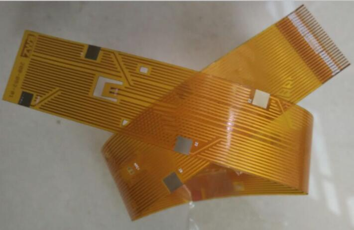
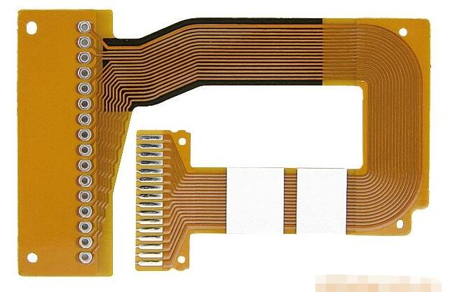
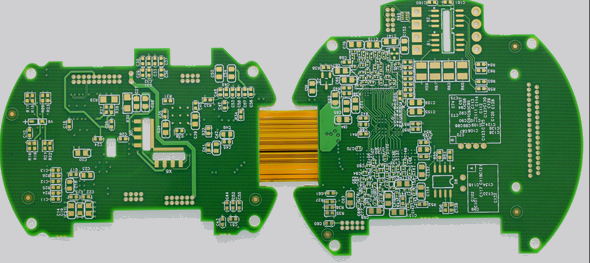
FPC process
2. Gold plated. As the name implies, gold plating is to spray a layer of gold on the surface of the substrate. Since there is no chemical combination of copper, the gold content on the surface is higher than that of the gold deposit, and the gold is brighter, but the welding effect is not as good as that of the gold deposit;
Advantages: Long storage time>12 months. Suitable for contact switch design and gold wire binding. Suitable for electrical testing
Weaknesses: high cost, relatively thick. Additional design wires are required for gold finger plating. Because the gold thickness is not always the same, when it is applied to welding, it may lead to embrittlement of solder joints due to too thick gold, affecting the strength. The uniformity of electroplating surface. Electroplated nickel gold does not cover the edge of the wire. Not suitable for aluminum wire binding.
3. Tin plating. Just like gold plating, tin is used instead of gold. The melting point of tin is not as high as gold, the hardness is not as high as gold, the color is poor, and the welding effect is good;
The general process of tin plating is: micro etching → preheating → coating flux → tin spraying → cleaning.
Advantages: Long storage time; After the PCB is completed, the copper surface is completely wetted (completely covered with tin before welding); Suitable for lead-free welding; Mature process, low cost, suitable for visual inspection and electrical testing
Disadvantages: Not suitable for wire binding; Due to the problem of surface flatness, there are also limitations on SMT; Not suitable for contact switch design. Copper will dissolve during tin spraying, and the plate will undergo a high temperature. For particularly thick or thin plates, tin spraying is limited and production operation is inconvenient.
4. OSP, namely oxidation prevention process. It is also a chemical method, which can avoid or slow down the oxidation of pads under certain circumstances. It is the most widely used process in FPC surface treatment except for gold deposition.
The general process is degreasing -->micro etching -->pickling -->pure water cleaning -->organic coating -->cleaning. Compared with other processes, process control indicates that the treatment process is relatively easy.
Advantages: simple process, very flat surface, suitable for lead-free welding and SMT. Easy rework, convenient production operation, suitable for horizontal line operation. The board is suitable for multiple processing (such as OSP+ENIG). Low cost and environment-friendly.
Disadvantages: limit of reflow times (the film will be damaged if the thickness is welded for many times, and there is basically no problem if it is welded twice). Not suitable for crimping technology, wire binding. Visual inspection and electrical measurement are inconvenient. N2 gas protection is required for SMT. SMT rework is not suitable. High requirements for storage conditions.
In terms of price, it is difficult to give an accurate price list due to the different manufacturing processes of FPCs.
The above is about the four common fpc flexible circuit board processes compiled by Xiao Bian. I hope it will be helpful to you. If there is still something unclear


Just upload Gerber files, BOM files and design files, and the KINGFORD team will provide a complete quotation within 24h.