
Professional PCB manufacturing and assembly
Building 6, Zone 3, Yuekang Road,Bao'an District, Shenzhen, China
+86-13410863085Mon.-Sat.08:00-20:00

Rigid flex joint plate, IC carrier plate and special electroplating method
Many customers often confuse the rigid flex joint plate and the IC carrier plate. Now let's ask the professional PCB manufacturer to explain the rigid flex joint plate and the IC carrier plate for you in detail?
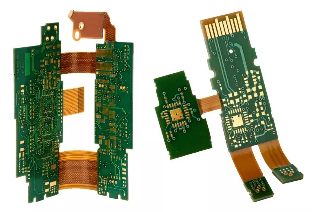
1. What is rigid flex joint plate?
Rigid flex bonding board refers to the combination of soft board and hard board. It is a circuit board formed by combining the thin layered flexible bottom layer and rigid bottom layer, and then pressing them into a single component. It is flexible and foldable. Due to the mixed use of a variety of materials and multiple manufacturing steps, the processing time of the rigid flex joint plate is longer and the manufacturing cost is higher.
In the PCB proofing of electronic consumer products, the use of rigid flex bonding plates not only maximizes the space use and minimizes the weight, but also greatly improves the reliability, thus eliminating many requirements for welding joints and fragile wiring prone to connection problems. The rigid flex composite plate also has high impact resistance and can survive in high stress environment.
The rigid flex joint plate is widely used in military, aviation and medical equipment, as well as in medical equipment such as pacemakers, to reduce its space and weight; At the same time, it is also widely used in various intelligent devices, testing equipment, mobile phones, digital cameras and automobiles.
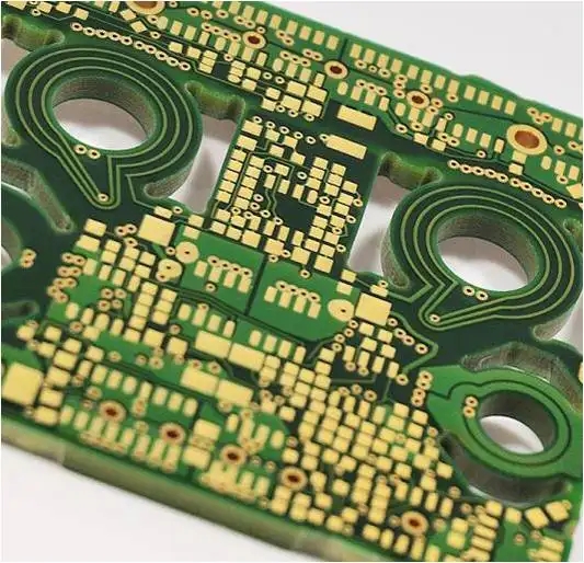
2. What is the IC carrier plate
IC carrier is a technology developed with the continuous progress of semiconductor packaging technology.
Like rigid flex joint plate, IC carrier plate belongs to high-end PCB board. It is developed on the basis of HDI board and has the characteristics of high density, high precision, miniaturization and thinness.
IC carrier is also called packaging substrate. In the field of high-order packaging, IC carrier has become an indispensable part of chip packaging. It not only provides support, heat dissipation and protection for chips, but also provides electronic connection between chips and PCB motherboards, playing a role of "connecting the preceding and the following"; It can even embed passive and active components to achieve certain system functions.
IC carrier products are roughly divided into five categories: memory chip IC carrier, MEMS IC carrier, RF module IC carrier, processor chip IC carrier and high-speed communication IC carrier, which are mainly used in mobile intelligent terminals, service/storage, etc.
What are the special electroplating methods in PCB electroplating
1、 Finger plating
In PCB proofing, rare metals are plated on the plate edge connector, plate edge protruding contact or gold finger to provide lower contact resistance and higher wear resistance, which is called finger plating or protruding local plating. The process is as follows:
1) Peel off the coating and remove the tin or tin lead coating on the protruding contact;
2) Water rinsing;
3) Scrub with abrasive;
4) The activation is submerged in 10% sulfuric acid;
5) Nickel plating thickness on protruding contact is 4-5 μ m;
6) Clean and remove mineral water;
7) Disposal of gold immersion solution;
8) Gold plating;
9) Cleaning;
10) Dry.
2、 Through-hole electroplating
There are many ways to set up a layer of electroplating layer that meets the requirements on the hole wall drilled on the substrate, which is called hole wall activation in industrial applications. The commercial consumption process of its printed circuit requires multiple intermediate storage tanks, and each storage tank has its own control and maintenance requirements. Through hole electroplating is a necessary subsequent manufacturing process in the drilling manufacturing process. When the drill bit drills through the copper foil and the substrate below it, the heat generated will cause the insulation synthetic resin that forms the majority of the substrate to condense. The condensed resin and other drilling debris will accumulate around the hole and be coated on the newly exposed hole wall in the copper foil. The condensed resin will also leave a layer of hot shaft on the hole wall of the substrate; Most of the activators show poor adhesion, which requires the development of a kind of technology similar to the chemical action of stain removal and corrosion back.
A more suitable method for PCB proofing is to use a specially designed low viscosity ink, which has a very strong adhesion and can be easily bonded to most hot polished hole walls, thus eliminating the step of back erosion.
3、 Roll linked selective plating
The pins and pins of electronic components, such as connectors, integrated circuits, transistors and flexible printed circuits, are all coated selectively to obtain good contact resistance and corrosion resistance. This plating method can be either manual or automatic. It is very expensive to select plating for each pin separately, so batch welding must be adopted. In choosing this electroplating method, first coat a layer of inhibitor film on the part of the metal copper foil that does not need electroplating, and only stop electroplating on the selected part of the copper foil.
4、 Brush plating
Brush plating is a kind of electrodeposition technology. It only stops electroplating in a limited area, and has no effect on other parts. Generally, rare metals are plated on selected parts of the printed circuit board, such as the board edge connector. Brush plating is used more frequently in electronic assembly workshops to repair discarded circuit boards.
Circuit board manufacturing, circuit board design, PCBA processing manufacturers will explain rigid flex joint plates, IC carrier plates and special electroplating methods.


Just upload Gerber files, BOM files and design files, and the KINGFORD team will provide a complete quotation within 24h.