
Professional PCB manufacturing and assembly
Building 6, Zone 3, Yuekang Road,Bao'an District, Shenzhen, China
+86-13410863085Mon.-Sat.08:00-20:00

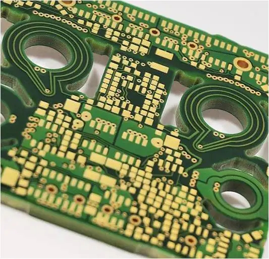
Reasons for copper rejection of PCB and shapes of pads used
In the manufacturing process of PCB, the copper wire of PCB often falls off, which is also known as copper throwing, thus affecting the product quality. So, what are the common reasons for copper rejection of PCB?
1、 PCB process factors:
Copper foil is excessively etched. The electrolytic copper foil used in the market is generally single-sided zinc plating (commonly known as ashing foil) and single-sided copper plating (commonly known as reddening foil). The common copper rejection is generally more than 70um of ashing foil. There is basically no batch copper rejection for reddening foil and less than 18um of ashing foil.
2. In PCB process, local collision occurs, and the copper wire is separated from the substrate by external mechanical force. This defect is characterized by poor positioning or orientation, and the detached copper wire will have obvious distortion, or scratches/impact marks in the same direction.
3. The PCB circuit design is unreasonable. If the circuit is designed too thin with thick copper foil, it will also cause excessive etching of the circuit and copper throwing.
2、 Reasons for laminate manufacturing process:
Under normal circumstances, as long as the high temperature section of the laminate is hot pressed for more than 30min, the copper foil and the prepreg will be basically bonded, so the bonding will not affect the bonding force between the copper foil and the substrate in the laminate generally. However, in the process of laminating and stacking, if PP is polluted or the rough surface of copper foil is damaged, the bonding force between copper foil and substrate after lamination will be insufficient, resulting in positioning (only for large plates) or sporadic copper wire falling off.
3、 Reasons for raw materials of laminate:
1. Ordinary electrolytic copper foil is the product that has been galvanized or coppered by the wool foil. If the peak value of the wool foil is abnormal during production, or the coating crystal branch is poor during galvanizing/copper plating, resulting in insufficient peel strength of the copper foil itself. When the defective foil is pressed into a PCB and inserted in the electronics factory, the copper wire will fall off under the impact of external forces.
2. Poor adaptability of copper foil and resin: when the copper foil is used in the production of laminate, it does not match the resin system, resulting in insufficient peeling strength of the metal foil covering on the sheet, and poor copper wire falling off during plug-in.
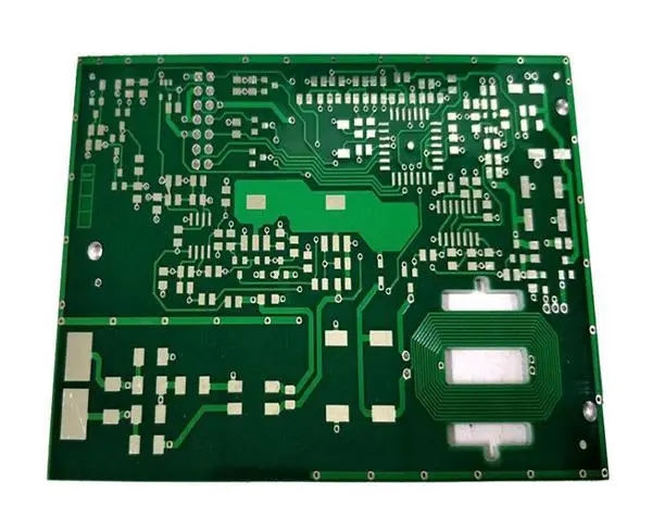
What are the shapes of pads used for printed circuit boards?
On the printed circuit board, the electrical connections of all components are made through bonding pads. According to different components and welding processes, pads can be divided into non via pads and via pads.
Non via pads are mainly used for welding surface mounted components, and via pads are mainly used for welding pin type components.
What shapes do pads have? Now, please follow the editor:
1. Round pad
In PCB proofing, round pad is the most commonly used pad. For via pads, the main dimensions of round pads are via size and pad size, and the pad size is generally twice the via size. Non through-hole round pad is mainly used for test pad, locating pad and reference pad, and its main size is pad size.
2. Rectangular pad
Rectangular pads are divided into square and rectangular pads. The square pad is mainly used to identify the first pin on the printed circuit board for installing components. The rectangular pad is mainly used as the pin pad of surface mount components. The pad size is related to the corresponding component pin size.
3. Octagonal pad
Octagonal pad is seldom used in PCB proofing. It is mainly set to meet the requirements of PCB wiring and bonding performance.
4. Special shaped pad
In PCB design, designers can use some special shaped pads according to the specific requirements of the design.
In a word, the selection of pad shape is related to the shape, size, layout, heating condition, force direction and other factors of components, and the designer needs to make the selection based on comprehensive consideration.
PCB manufacturers, PCB designers and PCBA manufacturers will explain the reasons for copper rejection of PCB and the shapes of pads used.


Just upload Gerber files, BOM files and design files, and the KINGFORD team will provide a complete quotation within 24h.