
Professional PCB manufacturing and assembly
Building 6, Zone 3, Yuekang Road,Bao'an District, Shenzhen, China
+86-13410863085Mon.-Sat.08:00-20:00

Electronic manufacturers explain how to copy and grind PCB?
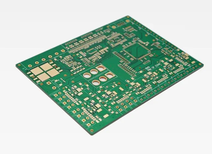
Generally, the fabrication method of multilayer board is to make the inner layer pattern first, then make a single or double sided substrate by printing and etching, and incorporate it into the designated interlayer, and then heat, pressurize and glue it. As for the later drilling, it is the same as the plating through hole method of double-sided board. It was invented in 1961.
In 1961, Hazelting Corp. of the United States published Multiplanar, which is the pioneer in the development of multilayer boards. This method is almost the same as the current method of manufacturing multilayer boards by plating through holes. After Japan stepped into this field in 1963, various conceptual schemes and manufacturing methods related to multilayer plates were gradually popularized all over the world. As the transistor has entered the era of integrated circuit, the application of computers has become more and more popular. Due to the demand for high functionality, large wiring capacity and good transmission characteristics have become the focus of the appeal of multilayer boards.
Selection of PCB Reading Software and Grinding Method
1. Selection of PCB copy software
The quality of PCB board reading software mainly depends on whether the functions are complete. It is better to do all the work in the PCB board reading software, so that the efficiency is high. It is best to support PROTEL99SE in component placement. Currently, 99SE has a very rich component library, which can be downloaded on the Internet. This is also a very important thing. The era of making components by hand has passed, because there are hundreds of elements in many BGP component packages. It is too expensive to build components by hand.
In order to ensure the stability and reliability of the circuit, a large piece of copper sheet should be connected to the power supply or ground when designing the circuit, which can reduce the noise and interference of the circuit. Therefore, the problem of copper laying on the network is involved. For complex circuit boards, there are many connections and many isolations on the copper laying. If this problem is not solved properly, copper laying cannot be realized. Therefore, we must define a network to lay copper ("the same network is connected, but different networks are isolated"). Simply filling all the copper sheets will lead to end circuits. This is also a key issue to measure PCB copy software.
2. Grinding plate
For multilayer boards, the middle layer cannot be scanned directly. If you want to copy multilayer boards, you must grind them out. Therefore, if you want to copy multilayer boards, you must scrap a PCB.
At present, the best method is to use a good grinder and manual gauze grinding. The latter method is the cheapest one. Abrasive paper is a common abrasive paper that can be purchased everywhere in the market. Remember to use coarse abrasive paper, while fine abrasive paper is difficult to grind.
The method is very simple. Grind the PCB board with sandpaper according to the right level. If there is a large piece of copper sheet, you can pull it off with pliers directly, or use a few flat blows to grind away the hard to grind, and then use sandpaper to grind again.
In fact, the grinding plate has no technical content. It is purely empirical. It can be understood by grinding a multilayer plate.


Just upload Gerber files, BOM files and design files, and the KINGFORD team will provide a complete quotation within 24h.