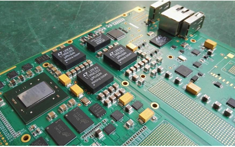
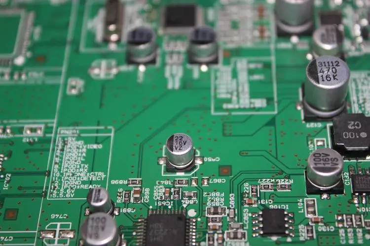
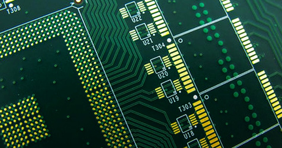
Ingenious Skills of PCB Layout and Treatment of Process Defects
This paper introduces the ingenious skills of PCB layout and the treatment of process defects in PCB design


This paper introduces the ingenious skills of PCB layout and the treatment of process defects in PCB design
This paper mainly introduces the method of false soldering and false soldering caused by improved PCB soldering in PCB chip processing
This article is about the method of optimizing the defect rate of automotive PCB in the testing process of automotive PCB enterprises
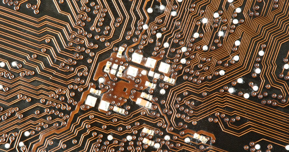
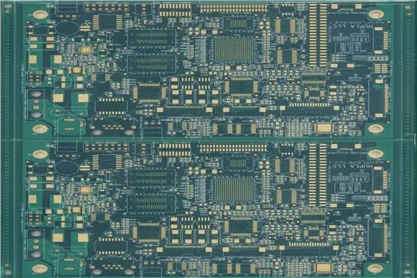
Understand PCB design, PCB layout and PCB manufacturing in PCB related industries, and Simply teach you how to complete the relevant design of PCB
Understand PCB design, PCB layout and PCB manufacturing in PCB related industries, and This is what people call complex PCB design rules

In 2022, PCBA electronic engineers must know the design criteria of high-frequency circuit printed boards
Which software do you usually use to draw schematic diagrams and PCBs?
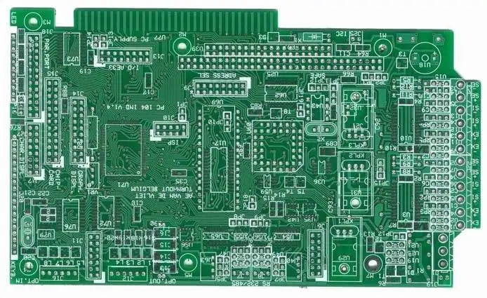
The small editor of Shenzhen PCB Factory explains the basic PCB design process for you
The small editor of Shenzhen PCB Factory explains the basic PCB design process for you

13 steps to detail the basic process of PCB design, from early preparation to project completion!
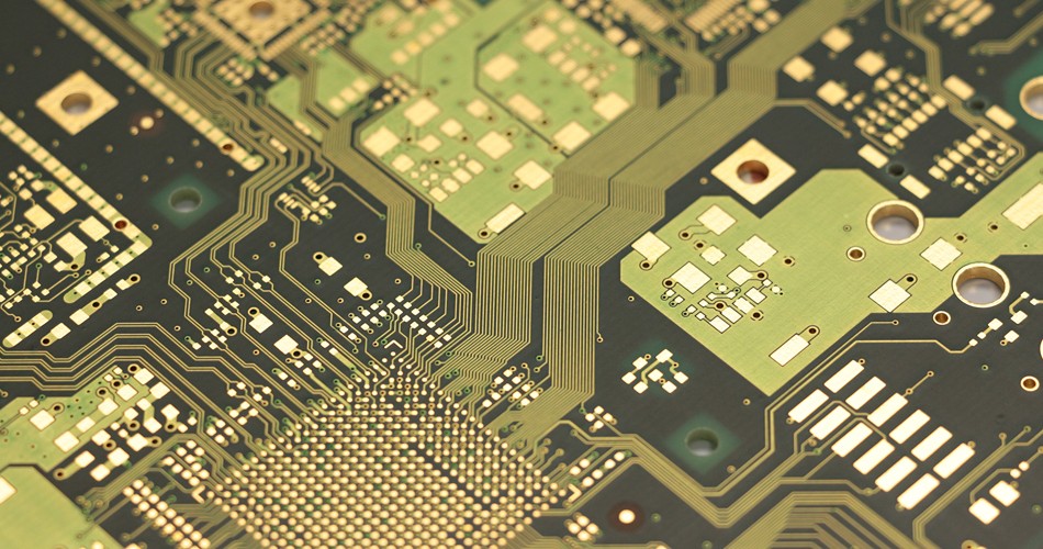
In 2022, PCB layout skills will be summarized, and you will be a hero again!
Shenzhen pcb factory explains pcb design stage precautions in detail


