
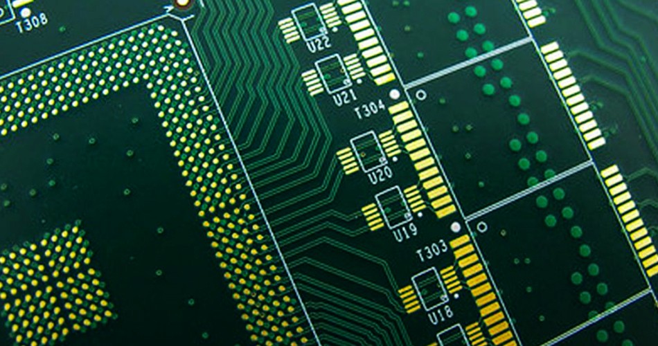
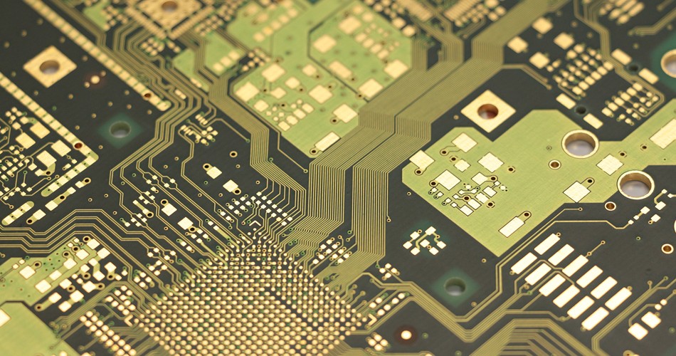
Professional PCB manufacturing and assembly
Building 6, Zone 3, Yuekang Road,Bao'an District, Shenzhen, China
+86-13410863085Mon.-Sat.08:00-20:00


General PCB basic design process is as follows:
Preliminary preparation → PCB structure design → guide network table → rule setting → PCB layout → wiring → wiring optimization and silk screen printing → network and DRC inspection and structure inspection → output photo drawing → photo drawing review → PCB board making production/proofing data → PCB board factory engineering EQ confirmation → chip mounting data output → project completion.
1: Preliminary preparation
This includes preparing package libraries and schematics. Before PCB design, first prepare the logic package of schematic SCH and the package library of PCB. The package library can be the library provided with PADS, but it is difficult to find a suitable one in general. It is better to make your own package library according to the standard size information of the selected components. In principle, the packaging library of PCB shall be built first, and then the logic packaging of SCH shall be built. PCB packaging library has high requirements, which directly affects the installation of boards; The logic packaging requirements of SCH are relatively loose. Just pay attention to defining the pin attributes and the corresponding relationship with PCB packaging. PS: Note the hidden pins in the standard library. After that, it is the schematic design. After that, it is ready to start PCB design.
2: PCB structure design
In this step, the PCB surface is drawn in the PCB design environment according to the determined PCB size and various mechanical positioning, and the required connectors, keys/switches, screw holes, assembly holes, etc. are placed according to the positioning requirements. And fully consider and determine the wiring area and non wiring area (such as how large the area around the screw hole belongs to the non wiring area).
3: Guide net list
It is recommended to import the board frame before the net guide table. Import frames in DXF format or emn format.
4: Rule Settings
Reasonable rules can be set according to the specific PCB design. What we call the rules is the constraint manager of PADS. The constraint manager restricts the line width and safety spacing at any link in the design process. The DRC Markers will be used to mark the areas that do not meet the constraints during subsequent DRC detection.
The general rule setting is placed before the layout because sometimes it is necessary to complete some fanout work during the layout. Therefore, the rules should be set before fanout. When the design project is large, the design can be completed more efficiently.
Note: Rules are set for better and faster design, in other words, for the convenience of designers.
General settings are:
1. Default line width/line spacing of common signal.
2. Select and set vias
3. Line width and color setting of important signals and power supplies.
4. Plate layer setting.
5: PCB layout
The general layout shall follow the following principles:
(1) According to the reasonable division of electrical performance, it is generally divided into: digital circuit area (i.e., fear of interference and generate interference), analog circuit area (fear of interference), power drive area (interference source);
(2) Circuits that complete the same function shall be placed as close as possible, and all components shall be adjusted to ensure the most concise connection; At the same time, adjust the relative position between the function blocks to make the connection between the function blocks the most concise;
(3) For components with high quality, the installation position and strength shall be considered; The heating element shall be placed separately from the temperature sensing element, and thermal convection measures shall be considered when necessary;
(4) The I/O driver shall be close to the edge of the printed board and the outlet connector as far as possible;
(5) The clock generator (such as crystal oscillator or clock oscillator) shall be as close as possible to the device using the clock;
(6) A decoupling capacitor shall be added between the power input pin of each integrated circuit and the ground (generally, a monolithic capacitor with good high-frequency performance is used); When the circuit board space is dense, a tantalum capacitor can also be added around several integrated circuits.
(7) Discharge diode (1N4148) shall be added at relay coil;
(8) The layout should be balanced, dense and orderly, not top heavy or heavy.
Special attention shall be paid to the actual size (area and height) of components and the relative position between components when placing components, so as to ensure the electrical performance of the circuit board and the feasibility and convenience of production and installation. At the same time, the placement of components shall be properly modified to make them neat and beautiful on the premise that the above principles can be reflected. Similar components shall be placed orderly and in the same direction, It should not be placed in an "orderly manner".
This step is related to the overall image of the board and the difficulty of wiring in the next step, so we should make great efforts to consider it. In the layout, preliminary wiring can be made for uncertain places, and full consideration can be given.
6: Wiring
Wiring is the most important process in PCB design. This will directly affect the performance of PCB. In the PCB design process, there are generally three levels of wiring:
The first is wiring, which is the most basic requirement for PCB design. If the lines are not connected and there are flying lines everywhere, it will be an unqualified board. It can be said that we haven't started yet.
The second is the satisfaction of electrical performance. This is the standard to measure whether a printed circuit board is qualified. This is to carefully adjust the wiring after wiring to achieve the best electrical performance.
Next is beauty. If your wiring is connected, there is no place that affects the performance of electrical appliances. But at a glance, it is chaotic, colorful and colorful. Even if your electrical performance is good, it is still a piece of garbage in the eyes of others. This brings great inconvenience to testing and maintenance. The wiring shall be neat and uniform, and shall not be crisscross and disorganized. All these should be achieved under the premise of ensuring the electrical performance and meeting other individual requirements, otherwise, it will be a waste of time.
The wiring shall be carried out according to the following principles:
(1) In general, the power line and ground wire shall be wired first to ensure the electrical performance of the circuit board. Within the allowable range, the width of power supply and ground wire shall be widened as much as possible. The ground wire is better than the power wire. Their relationship is: ground wire>power wire>signal wire. Generally, the width of signal wire is 0.2 ~ 0.3mm (about 8-12mil), the thinnest width can reach 0.05 ~ 0.07mm (2-3mil), and the power wire is 1.2 ~ 2.5mm (50-100mil). The PCB of digital circuit can be used to form a loop with a wide ground wire, that is, to form a ground grid for use (the ground of analog circuit cannot be used in this way).
(2) Wires with strict requirements (such as high-frequency lines) shall be wired in advance. The side lines of input and output terminals shall not be adjacent and parallel to each other to avoid reflection interference. If necessary, ground wires shall be added for isolation, and the wiring of two adjacent layers shall be perpendicular to each other, which may cause parasitic coupling.
(3) The oscillator shell shall be grounded, and the clock line shall be as short as possible, and shall not be led everywhere. The area of the ground under the clock oscillation circuit and special high-speed logic circuit should be added, and other signal lines should not be used to make the surrounding electric field approach zero;
(4) 45 ° broken lines shall be used as far as possible, and 90 ° broken lines shall not be used to reduce the radiation of high-frequency signals; (Double arc lines are also used for lines with high requirements)
(5) No signal line shall form a loop. If it is unavoidable, the loop shall be as small as possible; The vias of signal lines shall be as few as possible;
(6) The key lines shall be as short and thick as possible, and protective areas shall be added on both sides.
(7) When transmitting sensitive signals and noise field band signals through flat cables, they should be led out in the way of "ground wire signal ground wire".
(8) Test points shall be reserved for key signals to facilitate production, maintenance and detection
(9) After the schematic wiring is completed, the wiring shall be optimized; At the same time, after the preliminary network inspection and DRC inspection are correct, fill the ground wire in the unrouted area, use a large area of copper layer as the ground wire, and connect the unused places with the ground on the printed board as the ground wire. Or it can be made into multilayer boards, with one layer for power supply and one layer for ground wire.
PCB wiring process requirements (can be set in rules)
(1) Line
In general, the signal line width is 0.3mm (12mil), and the power line width is 0.77mm (30mil) or 1.27mm (50mil); The distance between lines and between lines and pads shall be greater than or equal to 0.33mm (13mil). In practical application, if conditions permit, the distance shall be increased;
When the wiring density is high, it can be considered (but not recommended) to use two lines between IC pins, the width of the line is 0.254mm (10mil), and the line spacing is not less than 0.254mm (10mil). Under special circumstances, when the device pins are dense and the width is narrow, the line width and line spacing can be appropriately reduced.
(2) Pads
The basic requirements for PAD and VIA are: the diameter of PAD is greater than that of hole by 0.6 mm; For example, universal pin resistors, capacitors, integrated circuits, etc., adopt 1.6mm/0.8mm (63mil/32mil) disk/hole size, 1.8mm/1.0mm (71mil/39mil) socket, pin, diode 1N4007, etc. In practical application, it shall be determined according to the size of the actual component. If possible, the pad size can be appropriately increased;
The component installation hole diameter designed on the PCB shall be 0.2~0.4mm (8-16mil) larger than the actual size of the component pin.
(3) Via (VIA)
Generally 1.27mm/0.7mm (50mil/28mil);
When the wiring density is high, the via size can be appropriately reduced, but should not be too small, and 1.0mm/0.6mm (40mil/24mil) can be considered.
(4) Spacing requirements for pads, wires and vias
PAD and VIA :≥ 0.3mm(12mil)
PAD and PAD :≥ 0.3mm(12mil)
PAD and TRACK :≥ 0.3mm(12mil)
TRACK and TRACK :≥ 0.3mm(12mil)
When the density is high:
PAD and VIA :≥ 0.254mm(10mil)
PAD and PAD :≥ 0.254mm(10mil)
PAD and TRACK :≥ 0.254mm(10mil)
TRACK and TRACK :≥ 0.254mm(10mil)
7: Routing optimization and silk screen
"There is no best, only better"! No matter how hard you try to design, after you finish painting, you will still feel that there are many places that can be modified. The general design experience is that the time for optimal routing is twice as long as the time for initial routing. I don't think there is anything that needs to be modified. After that, I can lay copper. Copper is generally laid with ground wire (pay attention to the separation of analog ground and digital ground), and power supply may also be required for multi-layer boards. For silk screen, it should be noted that it cannot be blocked by devices or removed by vias and pads. At the same time, when designing, face up to the component surface, and the characters at the bottom layer should be mirrored to avoid confusing the layers.
8: Network, DRC check and structure check
Before photo painting, it is generally necessary to check. Each company will have its own Check List, which contains the requirements of principle, design, production and other aspects.
9: Output photo
Before the photo output, it is necessary to ensure that the veneer is the latest version that has been completed and meets the design requirements. The photo output files are used for plate making in the plate factory, steel mesh making in the steel mesh factory, welding process documents in the welding factory, etc.
The output files are:
(1) Wiring layer: refers to the conventional signal layer, mainly wiring.
It is named L1, L2, L3, L4, where L represents the layer of the routing layer.
(2) Silk screen layer: refers to the layer in the design document that provides information for processing silk screen. Generally, if there are devices or marks on the top and bottom layers, there will be top and bottom silk screen.
Naming: the top layer is named SILK_ TOP ; The underlying layer is named SILK_ BOTTOM 。
(3) Soldering resistance layer: refers to the layer in the design document that provides processing information for green oil coating.
Naming: the top layer is named SOLD_ TOP; The underlying layer is named SOLD_ BOTTOM。
(4) Steel mesh layer: refers to the layer in the design document that provides processing information for solder paste coating. Generally, when there are SMD devices on the top layer and bottom layer, there will be steel mesh top layer and steel mesh bottom layer.
Naming: the top layer is named PASTE_ TOP ; The underlying layer is named PASTE_ BOTTOM。
(5) Drilling layer (including 2 files, NC DRILL NC drilling file and DRILL DRAWINGdrilling map)
They are named NC DRILL and DRILL DRAWINGrespectively.
10: Photo examination
After outputting photo, photo inspection, Cam350 open short circuit and other inspections should be carried out before sending it to the plate factory for plate making. In the later stage, attention should be paid to the plate making engineering and problem reply.
11: PCB board making data (Gerber photo drawing data+PCB board making requirements+assembly drawing)
12: PCB factory engineering EQ confirmation (board making engineering and question reply)
13: PCBA patch data output (steel grid data, patch tag number diagram, component coordinate file)
At this point, all the workflow of PCB design for a project is completed. PCB design is a very meticulous work, so we should be extremely careful and patient in design, and fully consider all factors, including production, assembly and processing, and ease of maintenance in the later period. In addition, develop some good work habits during design, which will make your design more reasonable, design more efficient, production easier, and performance better. When good design is applied to daily products, consumers will feel more confident and trust


Just upload Gerber files, BOM files and design files, and the KINGFORD team will provide a complete quotation within 24h.