
Professional PCB manufacturing and assembly
Building 6, Zone 3, Yuekang Road,Bao'an District, Shenzhen, China
+86-13410863085Mon.-Sat.08:00-20:00

Summary of PCB layout skills
PCB, also known as Printed Circuit Board, can realize the circuit connection and function realization between electronic components, and is also an important part of power circuit design. This article will introduce the basic rules of PCB layout and routing today.
Basic rules for component layout
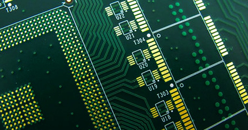
1. The layout shall be carried out according to the circuit modules. The relevant circuits that achieve the same function are called a module. The components in the circuit modules shall be centralized nearby, and the digital circuits and analog circuits shall be separated.
2. Elements and devices shall not be mounted within 1.27mm around non mounting holes such as positioning holes and standard holes, and components shall not be mounted within 3.5mm (for M2.5) and 4mm (for M3) around mounting holes such as screws.
3. Avoid laying vias under horizontally installed resistors, inductors (plug-ins), electrolytic capacitors and other components to avoid short circuit between vias and component shells after wave soldering.
4. The distance from the outer side of the components to the board edge is 5mm.
5. The distance between the outer side of the mounting element pad and the outer side of the adjacent plug-in elements is greater than 2mm.
6. The metal shell components and metal parts (shielding box, etc.) shall not collide with other components, and shall not be close to the printed wire and bonding pad. The distance between them shall be greater than 2mm. The distance from the outside of the positioning hole, fastener mounting hole, elliptical hole and other square holes in the plate to the plate edge is greater than 3mm.
7. The heating element shall not be close to the conductor and thermal element; High heat devices shall be evenly distributed.
8. The power socket shall be arranged around the printed board as much as possible, and the terminal of the power socket and its connected bus bar shall be arranged on the same side. Special attention shall be paid not to arrange power sockets and other welding connectors between connectors, so as to facilitate the welding of these sockets and connectors and the design and wiring of power cables. The spacing of power sockets and welding connectors shall be arranged to facilitate the plugging and unplugging of power plugs.
9. Layout of other components: All IC components are aligned on one side, and the polarity marks of polar components are clear. The polarity marks on the same printed board shall not be more than two directions. When there are two directions, the two directions are perpendicular to each other.
10. The wiring on the board surface shall be properly densified. When the density difference is too large, it shall be filled with mesh copper foil. The mesh shall be greater than 8mil (or 0.2mm).
11. There shall be no through-hole on the SMD pad to prevent the loss of solder paste from causing faulty soldering of components. Important signal wires are not allowed to pass through the socket pins.
12. The patch is aligned on one side, with consistent character direction and packaging direction.
13. Polarized devices shall be in the same direction as far as possible with polarity marks on the same board.
Component Routing Rules
1. No wiring is allowed in the area ≤ 1mm away from the PCB edge and 1mm around the mounting hole.
2. The power cord shall be as wide as possible and shall not be less than 18mil; The signal line width shall not be less than 12 mil; CPU incoming and outgoing lines shall not be less than 10mil (or 8mil); The line spacing shall not be less than 10mil.
3. Normal through-hole shall not be less than 30mil.
4. Double in-line insertion: pad 60ml, aperture 40ml.
L 1/4W resistance: 51 * 55mil (0805 meter sticker); The pad is 62mil and the hole diameter is 42mil during direct insertion.
L Stepless capacitance: 51 * 55mil (0805 meter sticker); The pad shall be 50 mil and the hole diameter shall be 28 mil during direct insertion.
5. Note that the power line and ground wire should be radial as far as possible, and the signal line should not be looped.
How to improve anti-interference ability and electromagnetic compatibility?
How to improve anti-interference ability and electromagnetic compatibility when developing electronic products with processors?
1. The following systems shall pay special attention to anti electromagnetic interference:
(1) The microcontroller has a very high clock frequency and a very fast bus cycle.
(2) The system contains high-power, high current drive circuits, such as spark generating relays, high current switches, etc.
(3) The system includes weak analog signal circuit and high-precision A/D conversion circuit.
2. The following measures shall be taken to increase the anti electromagnetic interference capability of the system:
(1) Microcontroller with low frequency shall be selected:
Microcontroller with low external clock frequency can effectively reduce noise and improve the anti-interference ability of the system. For square wave and sine wave with the same frequency, the high-frequency component in square wave is much more than that in sine wave.
Although the amplitude of the high-frequency component of the square wave is smaller than that of the fundamental wave, the higher the frequency, the easier it is to emit as a noise source. The influential high-frequency noise generated by the microcontroller is about three times the clock frequency.
(2) Reduce distortion in signal transmission
Microcontrollers are mainly manufactured with high-speed CMOS technology. The static input current of the signal input terminal is about 1mA, the input capacitance is about 10PF, and the input impedance is quite high. The output terminal of the high-speed CMOS circuit has a considerable load capacity, that is, a considerable output value. If the output terminal of a gate is led to the input terminal with a relatively high input impedance through a long line, the reflection problem is very serious, which will cause signal distortion and increase system noise. When Tpd>Tr, it becomes a transmission line problem, and signal reflection, impedance matching and other problems must be considered.
The delay time of the signal on the PCB is related to the characteristic impedance of the lead, that is, the dielectric constant of the PCB material. It can be roughly considered that the transmission speed of the signal in the PCB lead is about 1/3 to 1/2 of the speed of light. Tr (standard delay time) of common logic telephone elements in the system composed of microcontroller is between 3 and 18 ns.
On the printed circuit board, the signal passes through a 7W resistor and a 25cm long lead, and the line delay time is about 4~20ns. In other words, the shorter the lead of the signal on the printed line, the better, and the length should not exceed 25cm. And the number of vias shall be as small as possible, no more than 2.
When the rise time of the signal is faster than the signal delay time, it should be processed according to fast electronics. At this time, the impedance matching of the transmission line should be considered. For the signal transmission between the integrated blocks on a printed circuit board, the Td>Trd should be avoided. The larger the printed circuit board, the faster the system cannot be.
A rule of PCB design is summarized with the following conclusion: the delay time of signal transmission on PCB shall not be greater than the nominal delay time of the device used.
(3) Reduce cross interference between signal lines:
A step signal with rise time of Tr at point A is transmitted to end B through lead AB. The delay time of signal on AB line is Td. At point D, due to the forward transmission of point A signal, the signal reflection after arriving at point B and the delay of line AB, a page pulse signal with a width of Tr will be induced after Td time. At point C, due to the transmission and reflection of the signal on AB, a positive pulse signal with a width twice the delay time of the signal on AB line will be induced, that is, 2Td. This is the cross interference between signals.
The strength of the interference signal is related to the di/at of the C point signal and the distance between lines. When the two signal lines are not very long, what you see on AB is actually the superposition of two pulses.
The micro control made by CMOS process has high input impedance, high noise and high noise tolerance. The digital circuit does not affect its operation if it is superposed with 100-200mv noise. If line AB in the figure is an analog signal, such interference will become intolerable. If the printed circuit board is a four layer board, one of which is a large area of ground, or a double-sided board, and the reverse side of the signal line is a large area of ground, the cross interference between signals will be reduced.
The reason is that the characteristic impedance of the signal line is reduced in a large area, and the reflection of the signal at the D terminal is greatly reduced. The characteristic impedance is inversely proportional to the square of the dielectric constant of the medium between the signal line and the ground, and is proportional to the natural logarithm of the thickness of the medium.
If the AB line is an analog signal, the interference of the digital circuit signal line CD to AB should be avoided. There should be a large area of ground below the AB line, and the distance between the AB line and the CD line should be 2-3 times greater than the distance between the AB line and the ground. The local shielding ground can be used, and the ground wire can be laid on the left and right sides of the lead wire with the bonding.
(4) Reduce noise from power supply
The power supply not only provides energy for the system, but also adds its noise to the power supply. The reset line, interrupt line and other control lines of the microcontroller in the circuit are easy to be interfered by external noise.
The strong interference on the power grid enters the circuit through the power supply. Even in the battery powered system, the battery itself also has high-frequency noise. The analog signal in the analog circuit can not withstand the interference from the power supply.
(5) Pay attention to the high-frequency characteristics of printed wire boards and components
In the case of high frequency, the lead, via, resistance, capacitance, distributed inductance and capacitance of connectors on the printed circuit board cannot be ignored. The distributed inductance of capacitance and the distributed capacitance of inductance cannot be ignored.
The resistance will reflect the high-frequency signal, and the distributed capacitance of the lead will play a role. When the length is greater than 1/20 of the corresponding wavelength of the noise frequency, the antenna effect will be generated, and the noise will be transmitted outward through the lead.
The via of the printed circuit board causes a capacitance of about 0.6 pf. A 2-6pf capacitor is introduced into the packaging material of an integrated circuit itself. A connector on a circuit board has 520nH distributed inductance. A 24 pin integrated circuit block with double row straight cut is introduced with 4~18nH distributed inductor.
These small distributed parameters can be ignored in this low frequency microcontroller system; Special attention must be paid to high-speed systems.
(6) Element layout shall be reasonably divided
Anti electromagnetic interference shall be fully considered for the position of components arranged on the printed circuit board. One of the principles is that the lead wires between components shall be as short as possible. In terms of layout, the analog signal part, high-speed digital circuit part and noise source part (such as relay, large current switch, etc.) shall be reasonably separated, so that the mutual signals are coupled into.
Handle the grounding wire well: on the printed circuit board, the power line and ground wire are important. The main method to overcome electromagnetic interference is grounding.
For double-sided boards, the ground wire layout is particularly particular. By using the single point grounding method, the power and ground are connected to the printed circuit board from both ends of the power supply, with one contact for the power supply and one contact for the ground. There should be multiple return ground wires on the printed circuit board, which will converge to the contact of the return power supply, which is called single point grounding.
The so-called analog ground, digital ground and high-power device ground opening refers to that the wiring is separated and all are collected to this grounding point. Shielded cables are usually used to connect signals outside the printed circuit board. For high frequency and digital signals, both ends of the shielded cable are grounded. One end of the shielded cable used for low-frequency analog signal should be grounded.
Circuits that are very sensitive to noise and interference or circuits with high frequency noise especially serious should be shielded with metal covers.
(7) Use decoupling capacitor well
A good high-frequency decoupling capacitor can remove high-frequency components as high as 1GHz. Ceramic chip capacitors or multilayer ceramic capacitors have better high-frequency characteristics. When designing a printed circuit board, a decoupling capacitor should be added between the power supply and the ground of each integrated circuit.
The decoupling capacitor has two functions: on the one hand, it is the energy storage capacitor of the integrated circuit, providing and absorbing the charging and discharging energy of the integrated circuit at the moment of opening and closing the door; On the other hand, the high-frequency noise of the device is bypassed.
A typical decoupling capacitor with a decoupling capacitance of 0.1uf in a digital circuit has a 5nH distributed inductance, and its parallel resonance frequency is about 7MHz, which means that it has a good decoupling effect on noise below 10MHz, and has little effect on noise above 40MHz.
The parallel resonance frequency of 1uf and 10uf capacitors is above 20MHz, and the effect of removing high-frequency noise is better. It is often advantageous to have a 1uf or 10uf high-frequency capacitor where the power supply enters the printed board. Even battery powered systems need this capacitor.
One charge discharge capacitor, or storage discharge capacitor, shall be added for every 10 or so integrated circuits. The capacitor size can be 10uf. No electrolytic capacitor is used. The electrolytic capacitor is rolled up by two layers of thin film. This rolled up structure acts as an inductance at high frequencies, and uses a gallbladder capacitor or a polycarbonate brewing capacitor.
The decoupling capacitance value is not strictly selected, and can be calculated as C=1/f; That is, 0.1 uf is taken for 10MHz, and 0.1~0.01 uf can be taken for the system composed of microcontroller.
3. Some experience in reducing noise and electromagnetic interference.
(1) If you can use low-speed chips, you don't need high-speed ones. High speed chips are used in key places.
(2) A series of resistors can be used to reduce the jumping rate of the upper and lower edges of the control circuit.
(3) Try to provide some form of damping for relays, etc.
(4) Use a frequency clock that meets the system requirements.
(5) The clock generator shall be as close as possible to the device using the clock. The shell of quartz crystal oscillator shall be grounded.
(6) Circle the clock area with a ground wire and keep the clock wire as short as possible.
(7) The I/O drive circuit shall be as close to the edge of the printed board as possible, so that it can leave the printed board as soon as possible. The signal entering the PCB shall be filtered, and the signal coming from the high noise area shall also be filtered. At the same time, the serial terminal resistance shall be used to reduce the signal reflection.
(8) The useless end of MCD shall be connected high, or grounded, or defined as an output end. The power supply and ground terminals on the integrated circuit shall be connected, and shall not be suspended.
(9) The unused gate circuit input terminal shall not be suspended, the unused op amp positive input terminal shall be grounded, and the negative input terminal shall be connected to the output terminal.
(10) The printed board shall use 45 fold lines instead of 90 fold lines as far as possible to reduce the external transmission and coupling of high-frequency signals.
(11) The printed circuit board shall be partitioned according to the frequency and current switching characteristics, and the noise components shall be further away from the non noise components.
(12) Single point power supply and single point grounding, power line and ground wire shall be as thick as possible for single panel and double panel. If the economy is affordable, multi-layer boards shall be used to reduce the inductance of power supply and ground.
Explanation of general PCB basic design process
Oct 25,2022


Just upload Gerber files, BOM files and design files, and the KINGFORD team will provide a complete quotation within 24h.