
Professional PCB manufacturing and assembly
Building 6, Zone 3, Yuekang Road,Bao'an District, Shenzhen, China
+86-13410863085Mon.-Sat.08:00-20:00

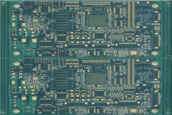
PCB factory: No.3: post wiring inspection stage
Digital analog
1. Whether the routing of digital circuit and analog circuit has been separated, and whether the signal flow is reasonable.
2. If the A/D, D/A and similar circuits are separated from the ground, whether the signal line between the circuits goes from the bridge point between the two grounds (except the differential line).
3. Signal lines that must cross the gap between split power supplies shall refer to the complete ground plane.
4. If the method of undivided stratigraphic design zoning is adopted, ensure that digital signals and analog signals are wired in zones.
Clock and high-speed part
1. Whether the impedance of each layer of high-speed signal line is consistent.
2. Whether the high-speed differential signal lines and similar signal lines are of equal length, symmetrical and parallel.
3. Make sure that the clock line is in the inner layer as far as possible.
4. Confirm whether the clock line, high-speed line, reset line and other strong radiation or sensitive lines have been wired according to the 3W principle as far as possible.
5. Whether there is no bifurcated test point on clock, interrupt, reset signal, 100M/Gigabit Ethernet and high-speed signal.
6. Whether low level signals such as LVDS and TTL/CMOS signals meet 10H as far as possible (H is the height of the signal line from the reference plane).
7. Whether the clock wire and high-speed signal wire avoid crossing the area with dense through-hole or wiring between device pins.
8. Whether the clock line has met the requirements (SI constraints) (whether the clock signal routing has achieved less vias, short routing and continuous reference planes, and the main reference plane should be GND as far as possible; if the GND main reference plane layer is changed during layer change, it is a GND vias within 200 mils from the vias; if the main reference planes of different levels are changed during layer change, whether there are decoupling capacitors within 200 mils from the vias).
9. Whether differential pairs, high-speed signal lines and various BUS have met the requirements (SI constraints).
EMC and Reliability
1. Whether a layer of ground is laid under the crystal oscillator; Whether the signal line is prevented from crossing the device pins; For high-speed sensitive devices, whether the signal line is prevented from passing through device pins.
2. The signal wiring of the single board shall not have acute angles or right angles (generally continuous turns are made at 135 degrees, and the RF signal wiring shall preferably be circular or chamfered copper foil after calculation).
3. For the double-sided board, check whether the high-speed signal line is wired closely with its return line; For multilayer boards, check whether the high-speed signal line is routed as close to the ground plane as possible.
4. For signal routing of two adjacent layers, try to route vertically.
5. Avoid signal lines crossing under power modules, common mode inductors, transformers and filters.
6. Try to avoid long-distance parallel routing of high-speed signals on the same layer.
7. Whether there are shielding vias at the dividing edges of digital ground, analog ground and protective ground on the board edge; Whether multiple ground planes are connected by vias; Whether the via distance is less than 1/20 of the wavelength of the highest frequency signal.
8. Whether the signal wiring corresponding to the surge suppression device is short and thick on the surface.
9. Confirm that the power supply and stratum are free of islands, excessive slotting, long ground surface cracks, thin strips and narrow channels caused by excessive or dense through-hole isolation panels.
10. Whether ground vias (at least two ground planes are required) are placed at places where signal lines cross more floors.
Power and ground
1. If the power/ground plane is divided, try to avoid high-speed signal crossing on the divided reference plane.
2. Confirm that the power supply and ground can carry enough current. Whether the number of vias meets the bearing requirements (estimation method: 1A/mm line width when the outer copper layer is 1oz thick, 0.5A/mm line width for the inner layer, and double the short line current).
3. For power supply with special requirements, whether the voltage drop requirements are met.
4. In order to reduce the edge radiation effect of the plane, the 20H principle should be met as far as possible between the power layer and the stratum (if conditions permit, the more the power layer is indented, the better).
5. If there is a ground division, whether the divided ground does not constitute a loop.
6. Whether overlapping placement is avoided for different power planes of adjacent layers.
7. Whether the isolation of protective ground, - 48V ground and GND is greater than 2mm.
8. Whether the - 48V ground is only the signal return of - 48V and not connected to other ground; If not, please explain the reason in the remark column.
9. Whether there is a 10~20mm protective ground near the panel with connectors, and each layer is connected with double row staggered holes.
10. Whether the distance between the power line and other signal lines meets the safety requirements.
Prohibited zone
1. There shall be no wiring, copper sheet and through hole that may cause short circuit under metal shell devices and radiator components.
2. There shall be no wiring, copper sheet and via that may cause short circuit around the mounting screws or washers.
3. Whether there is wiring in the reserved position in the design requirements.
4. The distance between the inner layer of the nonmetallic hole and the line and the copper foil shall be more than 0.5mm (20mil), the outer layer shall be 0.3mm (12mil), and the distance between the inner layer and the line and the copper foil shall be more than 2mm (80mil) for the single board pull wrench shaft hole.
5. Copper sheet and wire to plate edge are recommended to be more than 2mm and at least 0.5mm.
6. The copper sheet of the inner layer is 1~2 mm from the plate edge, and the minimum is 0.5 mm.
Pad outlet
1. For CHIP components (0805 and below packages) installed on two pads, such as resistors and capacitors, the printed wires connected to the pads should be symmetrically led out from the center of the pads, and the printed wires connected to the pads must have the same width. This provision can be ignored for outgoing wires with a line width less than 0.3mm (12mil).
2. The bonding pad connected with a wide printed wire should preferably be transited through a narrow printed wire (0805 and below).
3. The line shall be led out from both ends of the pad of SOIC, PLCC, QFP, SOT and other devices as far as possible.
Silk screen
1. Whether the device tag number is missing and whether the position can correctly identify the device.
2. Whether the device tag number meets the company's standard requirements.
3. Confirm the correctness of the pin arrangement order, the first pin mark, the polarity mark of the device and the direction mark of the connector.
4. Check whether the direction identifications of the plug-in boards of the parent board and the daughter board are corresponding.
5. Whether the backplane correctly identifies the slot name, slot number, port name and sheath direction.
6. Confirm whether the silk screen required by the design is added correctly.
7. Make sure that the anti-static and RF board signs have been placed (RF board is used).
Code/barcode
1. Confirm that the PCB code is correct and complies with the company's specifications.
2. Confirm that the PCB coding position and layer of the board are correct (it should be on the top left of side A, the silk screen layer).
3. Confirm that the PCB coding position and layer of the backplane are correct (it should be on the upper right side of B and the outer copper foil surface).
4. Confirm that there is a bar code laser printed white silk screen marking area.
5. Make sure that there is no connecting line or through hole larger than 0.5mm under the barcode frame.
6. Confirm that no components with a height of more than 25 mm can be found within 20 mm outside the white screen area of the barcode.
Through-hole
1. On the reflow soldering surface, the vias cannot be designed on the pad (the spacing between the vias of the normally opened window and the pad should be greater than 0.5mm (20mil), and the spacing between the vias covered with green oil and the pad should be greater than 0.1mm (4mil). The method is to open the Same Net DRC, check the DRC, and then close the Same Net DRC).
2. The arrangement of vias should not be too dense to avoid large-scale fracture of power supply and ground plane.
3. The hole diameter of the drilled hole should be no less than 1/10 of the plate thickness.
workmanship
1. Whether the device deployment rate is 100%, and whether the deployment rate is 100% (if not, please specify in the remarks).
2. Whether the Dangling line has been adjusted to the minimum, and the reserved Dangling lines have been confirmed one by one.
3. Whether the process problems fed back by the Process Department have been carefully checked.
Large area copper foil
1. For the large area copper foil on the top and bottom, if there is no special need, grid copper shall be used (diagonal mesh for veneer, orthogonal mesh for backplane, line width 0.3mm (12 mils), spacing 0.5mm (20mil)).
2. The component pad in the large copper foil area shall be designed as a rosette pad to avoid false soldering; When there is a requirement for current, the reinforcement of the rosette pad shall be widened first, and then the full connection shall be considered.
3. When distributing copper in a large area, try to avoid dead copper (isolated island) without network connection.
4. Pay attention to whether there is illegal connection and unreported DRC for large area copper foil.
Test point
1. Whether the test points of various power supplies and grounds are sufficient (at least one test point is available for every 2A current).
2. It is confirmed that the networks without test points can be simplified after confirmation.
3. Confirm that no test points are set on plug-ins that are not installed during production.
4. Whether the Test Via and Test Pin have been fixed (applicable to the modification of the test needle bed).
DRC
1. The spacing rule of Test via and Test pin should be set to the recommended distance first to check the DRC. If there is still DRC, check the DRC with the minimum distance setting.
2. Set the open constraint to the open status, update the DRC, and check whether there are disallowed errors in the DRC.
3. Confirm that DRC has been adjusted to the minimum, and confirm that DRC cannot be eliminated one by one.
Optical anchor point
1. Confirm that the PCB surface with mounting components has optical positioning symbols.
2. Confirm that the optical positioning symbol is not crimped (silk screen and copper foil routing).
3. The background of the optical positioning point shall be the same, and the distance between the center and the edge of the optical point used for the whole board shall be ≥ 5mm.
4. Confirm that the optical positioning reference symbol of the whole board has been assigned a coordinate value (it is recommended to place the optical positioning reference symbol in the form of a device), and it is an integer value in millimeters.
5. For IC with pin center distance less than 0.5mm and BGA device with center distance less than 0.8mm (31 mil), optical positioning points shall be set near the diagonal of the element
Resistance welding inspection
1. Confirm whether all pads with special requirements are opened correctly (pay special attention to hardware design requirements).
2. Whether the vias under BGA are treated as oil plug holes.
3. Whether small windows or oil plug holes have been opened for vias other than test vias.
4. Whether the window opening of the optical positioning point avoids copper exposure and wire exposure.
5. Whether the power supply chip, crystal oscillator and other devices that need copper skin for heat dissipation or grounding shielding have copper skin and open the window correctly. The devices fixed by soldering tin shall have green oil to block the large area diffusion of soldering tin.
Borehole map
1. Whether the PCB thickness, layers, screen color, warpage and other technical specifications in Notes are correct.
2. Whether the layer name, stacking sequence, medium thickness and copper foil thickness of the lamination diagram are correct; Whether impedance control is required and whether the description is accurate; Whether the layer name of the stacked plate drawing is consistent with its photo file name.
3. Turn off the Repeat code in the setting table, and the drilling accuracy should be set to 2-5.
4. Whether the hole table and drilling files are up to date (when changing holes, they must be regenerated).
5. Whether there is abnormal hole diameter in the hole table, and whether the hole diameter of crimping parts is correct; Whether the hole diameter tolerance is marked correctly.
6. Whether the vias to be plugged are listed separately and marked with "filled vias".
Light painting
1. The photo file output should adopt the RS274X format as far as possible, and the precision should be set to 5:5.
2、art_ aper. Whether txt is up to date (274X can be unnecessary).
3. Whether there is an exception report in the log file of the output photo file.
4. Edge and island confirmation of negative film layer.
5. Use the photo inspection tool to check whether the photo file is consistent with the PCB (use the comparison tool to compare the modified board).
Complete set of documents
1. PCB file: product model_ Specifications_ Board code_ Version number. brd.
2. Backing plate design document: product model_ Specifications_ Board code_ Version No. - CB [- T/B]. brd.
3. PCB processing file: PCB code.zip (including photo file, aperture table, drilling file and ncdrill.log of each layer; panel also needs panel file *. dxf provided by the process), and backplane also needs to attach backing plate file: PCB code-CB [- T/B]. zip (including drill.art, *. drl, ncdrill. log).
4. Process design document: product model_ Specifications_ Board code_ Version number - GY.doc.
5. SMT coordinate file: product model_ Specifications_ Board code_ Version No. - SMT Txt (When outputting coordinate files, confirm to select Body center. Symbol origin can be selected only when confirming that the origin of all SMD device libraries is the device center).
6. PCB structure file: product model_ Specifications_ Board code_ Version No. - MCAD.zip (including. DXF and. EMN files provided by the structural engineer).
7. Test document: product model_ Specifications_ Board code_ Version No. - TEST.ZIP (contains the coordinate files of testprep.log and untest.lst or *. drl test points).
8. Archive drawing documents: product model and specification - board name - version number Pdf (including: front cover, home page, silk screen of each layer, circuit of each layer, drilling drawing, drawing of backing plate included in the back plate).
Standardization
1. Confirm that the information on the cover and front page is correct.
2. Confirm that the drawing serial number (corresponding to the sequence assignment of each PCB layer) is correct.
3. Confirm that the PCB code on the drawing frame is correct.

Summary of PCB layout skills
Oct 25,2022


Just upload Gerber files, BOM files and design files, and the KINGFORD team will provide a complete quotation within 24h.