
Professional PCB manufacturing and assembly
Building 6, Zone 3, Yuekang Road,Bao'an District, Shenzhen, China
+86-13410863085Mon.-Sat.08:00-20:00

Is PCB design complex? Unexpected factors often affect the implementation of the overall solution. How can we overcome these different problems? How do we draw clean, efficient and reliable PCB boards? We are a professional pcb design company, let's take a look today.
PCB board design seems very complicated. It is necessary to consider the direction and energy transmission of various signals. But in fact, the summary is very clear, which can be started from two aspects:
Frankly speaking, it is: "how to connect it" and "how to connect it".
1. Follow the layout principle of "large first, small first, difficult first", that is, important unit circuits and core components should be given priority. This is just like eating a buffet: the appetite of the buffet is limited to selecting the favorite food, while the PCB design space is limited to selecting important pendulums.
2. The layout shall refer to the schematic block diagram and arrange the main PCB components according to the main signal flow direction designed by the pcb board. PCB layout shall meet the following requirements as far as possible: the total connection shall be as short as possible, and the key signal line shall be as short as possible; The decoupling capacitor shall be arranged as close as possible to the power supply pin of the IC, and the loop formed between the power supply and the ground shall be as short as possible; Run to prevent accidents on the road.
3. The arrangement of components should be easy to debug and repair, that is, there should be no large components around small components, and there must be enough space around the components to be debugged, and overcrowding often becomes very embarrassing.
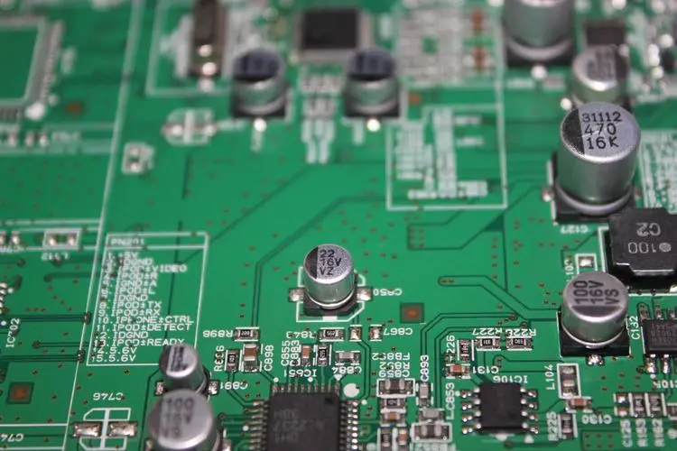
As shown in Figure 4, the heating elements should be roughly evenly distributed. In order to facilitate the heat dissipation of the single board and the whole machine, the temperature sensing elements other than the temperature detection elements should be far away from the elements with high heat.
5. "Symmetrical" standard layout shall be adopted as far as possible for the circuit part of the same structure; Optimize the layout according to the standard of uniform distribution, balance of gravity and beautiful layout.
6. Plug in components of the same type shall be placed in one direction along the X or Y direction. The same type of polar discrete components must also be consistent in the X or Y direction to facilitate production and inspection.
7. High voltage and high current signals are separated from low current and low voltage weak signals; Separation of analog signal and digital signal; Separation of high frequency signal and low frequency signal; The spacing of high-frequency components is sufficient. When dealing with PCB components, it should be considered that the equipment using the same power supply should be put together as much as possible to facilitate future power separation.
The above are the main considerations for "how to place" layout. And "how to connect" is relatively more complex, generally speaking:
Priority of key signal lines: simulate priority routing of key signals, such as small signals, high-speed signals, clock signals and synchronization signals;
Density priority principle: start wiring from the most complex equipment of pcbboard design. Wiring from the densest area of the circuit board.


Just upload Gerber files, BOM files and design files, and the KINGFORD team will provide a complete quotation within 24h.