Professional PCB manufacturing and assembly
Building 6, Zone 3, Yuekang Road,Bao'an District, Shenzhen, China
+86-13923401642Mon.-Sat.08:00-20:00
PCB Design

PCB Design

Six Skills for Selecting Components in Circuit Board Design
30Oct
Andy 0 Comments

Six Skills for Selecting Components in Circuit Board Design

The circuit board manufacturer and the circuit board designer will explain the six techniques for selecting components in circuit board design

Anti interference Design of High Frequency Circuit Board
30Oct
Andy 0 Comments

Anti interference Design of High Frequency Circuit Board

The circuit board manufacturer and circuit board designer explain the anti-interference design of high-frequency circuit boards

Basic principles and precautions of circuit board design
30Oct
Andy 0 Comments

Basic principles and precautions of circuit board design

The circuit board manufacturer and circuit board designer explain the basic principles of circuit board design

Code for circuit board design of switching power supply
30Oct
Andy 0 Comments

Code for circuit board design of switching power supply

The circuit board manufacturer and circuit board designer explain the circuit board design specifications of switching power supply

Design for Manufacturability of Through Hole Plug in PCB  ​
29Oct
Jeff 0 Comments

Design for Manufacturability of Through Hole Plug in PCB ​

This paper introduces some DFM methods related to PCB through-hole insertion in PCB production

Wiring arrangement and reasonable layout of components on PCB
29Oct
Jeff 0 Comments

Wiring arrangement and reasonable layout of components on PCB

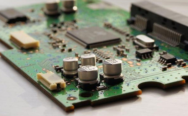
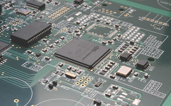
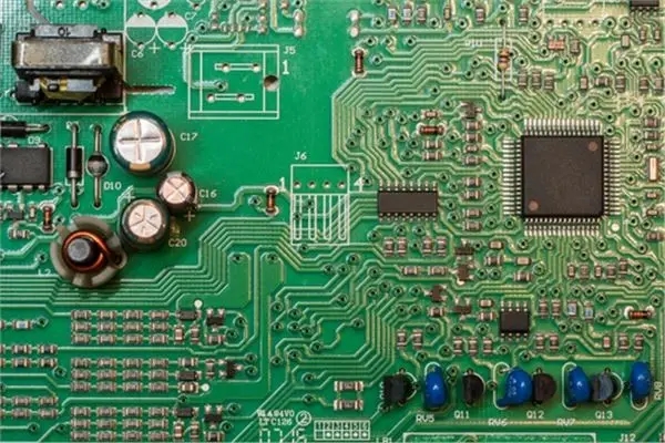
Introduction to the wiring arrangement and reasonable layout of PCB devices on the PCB board

Design method of multilayer board
29Oct
Caddy 0 Comments

Design method of multilayer board

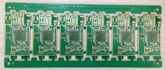
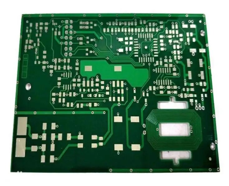
Multilayer and double-layer panels are similar in design for easier wiring. First of all, the layered structure should be divided, with the substrate as the center and symmetrically distributed on both sides, and the adjacent signal layers should be separ

How to design appropriate FPC FPC FPC and identify FPC FPC
29Oct
Summer 0 Comments

How to design appropriate FPC FPC FPC and identify FPC FPC

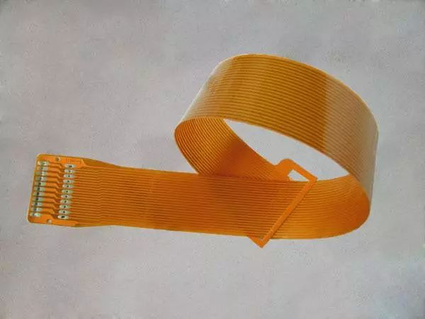
This paper mainly introduces the design of appropriate FPC flexible circuit board and the identification of FPC circuit board

Perfect combination of circuit electronic products and PCB board design
28Oct
Jeff 0 Comments

Perfect combination of circuit electronic products and PCB board design

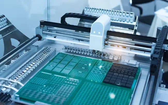
Understand PCB design, PCB products and PCB manufacturing in PCB related industries, and Perfect combination of circuit electronic products and PCB board design

What are the advantages of FPC
27Oct
Summer 0 Comments

What are the advantages of FPC

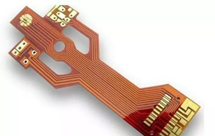
This article mainly introduces what advantages FPC has to be so popular

PCBA "three prevention" process design explanation
27Oct
Andy 0 Comments

PCBA "three prevention" process design explanation

PCB manufacturer explains PCBA "three prevention" process design

PCB design and anti deformation design
27Oct
Andy 0 Comments

PCB design and anti deformation design

PCB manufacturers explain the points needing attention in PCB design and anti deformation design

Just upload Gerber files, BOM files and design files, and the KINGFORD team will provide a complete quotation within 24h.