
Professional PCB manufacturing and assembly
Building 6, Zone 3, Yuekang Road,Bao'an District, Shenzhen, China
+86-13410863085Mon.-Sat.08:00-20:00

PCB design and anti deformation design
The domestic research on the automatic detection system of printed circuit board started in the middle school of the 1990s, and has just started. There are few research institutes engaged in this field, and because of the influence of various factors, the research on automatic optical detection system for PCB defects also stays at a relatively early level. Because the automatic detection system for printed circuit boards in foreign countries is too expensive, and there is no real automatic detection equipment for printed circuit boards in China, most domestic manufacturers of printed circuit boards still use manual magnifier or projector for inspection. Due to the labor intensity of manual inspection, eyes are prone to fatigue, and the rate of missed inspection is very high. Moreover, with the development of electronic products towards miniaturization and digitalization, printed circuit boards are also developing towards high-density and high-precision. It is basically impossible to use manual inspection methods. For circuit boards with higher density and precision (0.12-0.10mm), it is impossible to inspect them. Due to the backwardness of detection methods, the qualification rate of domestic multilayer boards (8-12 layers) is only 50~60%.
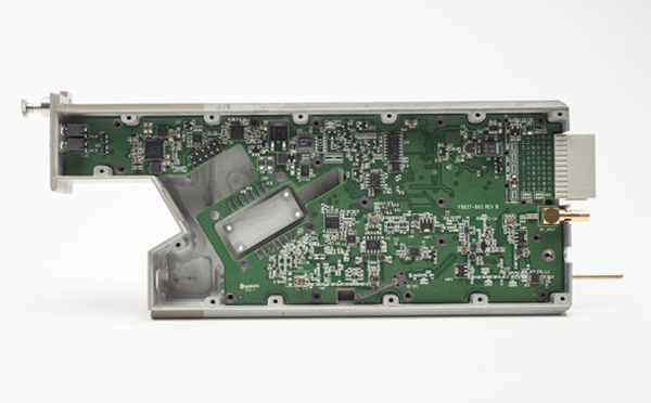
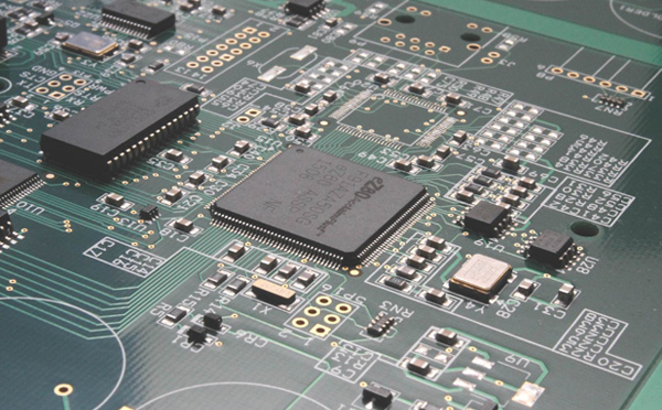
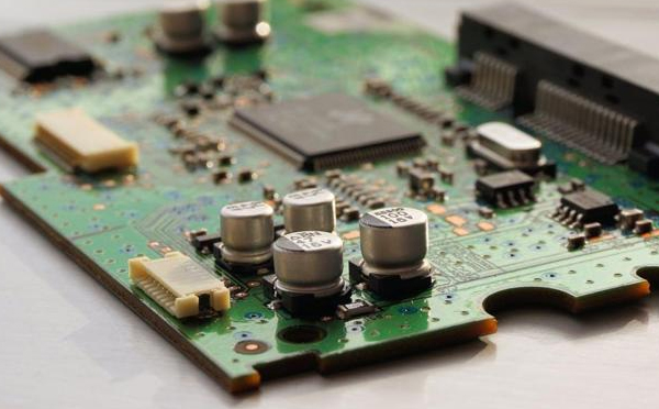
PCB Layout refers to PCB layout. In order to obtain the best performance of electronic circuits, the layout of electronic components and the wiring of wires are very critical. To make PCB have good quality, low cost and high performance, the design should focus on the layout link. The following are the principles of PCB layout:
In PCB design, first of all, we should fully consider the factors of PCB size. PCB size affects the performance of PCB. We need to design different PCB sizes according to the actual situation and the needs of PCB, then determine the PCB, then determine the location of special components, and finally layout all circuit components according to the functions required by the circuit.
Special electronic components generally refer to the key components in the high-frequency part, the core components in the circuit, the high-voltage electronic components, etc. Analysis of the location of special electronic components is the key to PCB layout. PCB layout that meets the requirements of circuit functions and production needs should be well done. Inappropriate placement of special electronic components or causes circuit compatibility problems, affects signal integrity, etc., leading to the failure of PCB design.
1. Shorten the connection between high-frequency components as much as possible, and strive to reduce the distribution parameters and electromagnetic interference of high-frequency components
2. The electronic components vulnerable to interference shall not be placed too close, and the input and output terminals shall be as far away as possible
3. Some electronic components or wires have high potential difference. The distance between them should be increased to avoid short circuit problems. High voltage electronic components should be placed in places that are difficult to reach.
4. The electronic components with a weight of more than 15g shall be fixed and welded with brackets. The electronic components with heavy and high temperature characteristics need to consider heat dissipation in advance and should be placed on the bottom plate of the main box.
5. Thermal elements shall be far away from heating elements
6. The layout of adjustable components shall fully consider the structural requirements of the whole PCB
7. The commonly used switches should be placed at the things easy to touch
In general, PCB layout should strive to achieve balanced performance and density.
1. What is PCB deformation?
PCB deformation, also known as warpage, has a great impact on welding and use. Especially for communication products, the single board is installed in a plug-in box. There is a standard spacing between the plug-in boards. With the narrowing of the panel, the gap between the components on the adjacent plug-in boards becomes smaller and smaller. If the PCB is bent, it will affect the insertion and removal during the electronic processing, and will touch the components. On the other hand, PCB deformation has a great impact on the reliability of BGA components. Therefore, it is very important to control PCB deformation during and after welding.
2. PCB anti deformation design requirements
(1) The deformation degree of PCB is directly related to its size and thickness. Generally, length width ratio ≤ 2, width thickness ratio ≤ 150.
(2) Multilayer rigid PCB is composed of copper foil, semi curing sheet and core board. In order to reduce the deformation after pressing, the laminated structure of PCB shall meet the requirements of symmetry design, that is, the thickness of copper foil, the category and thickness of media, the category of graphic distribution (circuit layer, plane layer), and the pressing property shall be symmetrical with respect to the centerline of the PCB thickness direction.
(3) For large size PCB, anti deformation reinforcing rib or lining plate (also known as fireproof plate) shall be designed, which is a mechanical reinforcement method.
(4) For locally installed structural parts that are easy to cause PCB deformation, such as CPU card holder, PCB deformation resistant liner shall be designed.


Just upload Gerber files, BOM files and design files, and the KINGFORD team will provide a complete quotation within 24h.