
Professional PCB manufacturing and assembly
Building 6, Zone 3, Yuekang Road,Bao'an District, Shenzhen, China
+86-13410863085Mon.-Sat.08:00-20:00

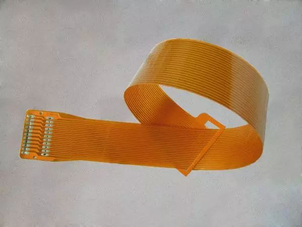
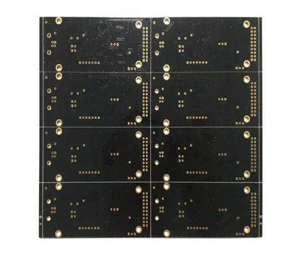
FPC circuit board can be divided into single panel, double panel, multilayer board, soft and hard combination board and special process board according to the structure required by industrial production. Single panel, also known as single-layer board, is the simplest FPC soft board, which is generally composed of base material+covering film+copper foil+transparent adhesive. The copper foil needs to be etched to obtain the required circuit, and the protective film needs to be drilled to expose the corresponding bonding pad. After cleaning, press the two together with pressing. Then, the exposed bonding pad shall be electroplated with gold or tin for protection. In this way, the big board is ready. Generally, small circuit boards should be stamped into corresponding shapes. There are also those who print solder mask directly on copper foil without using protective film. This will lower the cost, but the mechanical strength of the circuit board will become worse. Unless the strength requirement is not high but the price needs to be as low as possible, it is better to apply the protective film. Since there are too many lines required for dual panel, it is impossible to lay all the required lines on one board. Then lay the remaining lines on the other FPC board and press the two boards together. When we get a double-sided board, we can see that there are lines on both sides of it. This is the double-sided board. Because of the advent of high-frequency dielectric substrate in the 1990s, FPC circuit board has been leapfrog development, making FPC circuit board is no longer limited to single-sided, double-sided. Instead, multilayer FPC circuit boards can be pressed into one piece, and multilayer boards are more than one type of capacitive circuit board. Now the most widely used are multilayer boards and soft and hard combination boards. The soft and hard combination board is to make the circuit board have both the flexibility of FPC and the rigidity of PCB. It is the advantage combination board of soft board and hard board. The soft and hard combination board is the most widely used in today's applications. The special FPC process board can be divided into two types: surface treatment and shape treatment. The surface treatment methods include gold deposition, anti oxidation, gold plating, tin spraying, etc. Generally, because the special circuit board has higher requirements than the general circuit board, the special treated circuit board is more high-end than the general circuit board in the industry in general application. The reason for shape treatment is that the shape of electronic products has been set, and the embedded space left for the circuit board is fixed, so it is required to conduct shape treatment for the circuit board. The treatment methods include manual shape treatment, CNC machine tool cutting, and laser cutting.

According to the combination mode of base material and copper foil, it can be divided into adhesive calendered soft board and non adhesive calendered soft board. Among them, the adhesive free soft board can be more flexible than the adhesive free soft board, and can be wound and bent more vigorously than the adhesive free soft board. The parameters in all aspects are better than those with glue, but the price is higher and the defective rate is higher, which is generally applicable to high-end precision industries.
How to design the most suitable FPC circuit board? On this point, we can distinguish it mainly by whether it is manual wiring.
How to Design Suitable FPC
Method 1: Non manual wiring
Since it is not manual wiring, it is automatic wiring. This method mainly includes the following steps:
1. Use the schematic editor to design the schematic diagram, conduct electrical inspection (ERC) and generate the network table of the schematic diagram;
2. Enter the circuit board environment, and use the circuit wizard to determine the circuit board parameters such as the number of layers and size of the circuit board;
3. After the network table is called, the components are reasonably distributed on the circuit board.
4. After that, you can set automatic routing rules and route automatically.
Method 2: Manual wiring
Unlike automatic wiring, manual wiring is mainly manual. First, we need to ensure the level and size of the circuit board;
2. Packaging of self placed components and packaging of placement components;
3. After that, the wiring can be done according to the schematic diagram of the circuit board, and the circuit board can be modified, saved or printed;
4. Complete the wiring.
Through the above two completely different wiring methods, we can complete the basic wiring layout of the FPC.
Design method of multilayer board
Oct 29,2022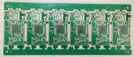


Just upload Gerber files, BOM files and design files, and the KINGFORD team will provide a complete quotation within 24h.