
Professional PCB manufacturing and assembly
Building 6, Zone 3, Yuekang Road,Bao'an District, Shenzhen, China
+86-13410863085Mon.-Sat.08:00-20:00

Discussion on Welding Defects of PCB
When the circuit board is being welded, defects often occur, such as faulty soldering, solder accumulation, too much solder, too little solder, rosin soldering, overheating, cold soldering, and poor wetting. So, apart from what we just said, what are the defects? Let me explain for you:
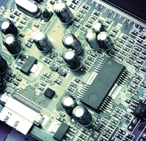
PCB circuit board

1. Asymmetrical: Solder is not full of pads.
Hazard: insufficient strength.
reason:
1) The fluidity of solder is poor.
2) Insufficient flux or poor quality.
3) Insufficient heating.
2. Loose: The lead wire or component lead can be moved.
Hazard: poor or no continuity.
reason:
1) The lead wire moves before the solder is solidified, causing the gap.
2) The lead wire is not well treated (poor or not soaked).
3. Tip: A tip appears.
Hazard: poor appearance, easy to cause bridging.
reason:
1) Too little flux and too long heating time.
2) The withdrawal angle of soldering iron is improper.
4. Bridging: connection of adjacent conductors.
Hazard: electrical short circuit.
reason:
1) Too much solder.
2) The withdrawal angle of soldering iron is improper.
5. Pinhole: hole is visible through visual inspection or low-power amplifier.
Hazard: the strength is insufficient, and the welding spot is easy to corrode.
Cause: The clearance between the lead wire and the pad hole is too large.
6. Bubble: there is a flame spraying solder bulge at the root of the lead, and there is a cavity inside.
Hazard: temporary conduction, but it is easy to cause poor conduction for a long time.
reason:
1) The gap between the lead wire and the pad hole is large.
2) The lead wire is poorly infiltrated.
3) The welding time of double-sided plate plug through-hole is long, and the air in the hole expands.
7. Copper foil cocking: copper foil is stripped from the printed board.
Hazard: The printed board is damaged.
Cause: The welding time is too long and the temperature is too high.
8. Peeling: Solder joints are peeled off from copper foil (not from copper foil and printed circuit board).
Hazard: causing open circuit.
Cause: poor metal coating on the pad.
The above is the explanation given by the editor of pcb circuit board company. If you want to know more about PCBA, you can go to our company's home page to learn about it. In addition, our company also sells various circuit boards,
High frequency circuit board and SMT chip are waiting for your presence again.


Just upload Gerber files, BOM files and design files, and the KINGFORD team will provide a complete quotation within 24h.