
Professional PCB manufacturing and assembly
Building 6, Zone 3, Yuekang Road,Bao'an District, Shenzhen, China
+86-13410863085Mon.-Sat.08:00-20:00


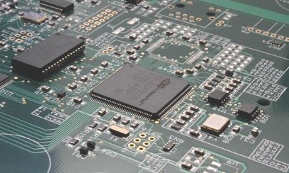
The important influence of PCB design on printed boards determines the manufacturing, installation and later maintenance costs of printed boards to some extent. In the trend of high density of electronic design, PCB layout and wiring of each electronic product is particularly important. Good PCB circuit board layout design can often achieve a higher rate of transmission, reduce the distribution of jumpers and electromagnetic interference between wires. Effectively reduce the generation of noise. The PCB design of the control board should follow the following principles:
One, in terms of the layout of components, the components related to each other should be placed as close as possible. For example, the clock generator, crystal oscillator and CPU clock input are easy to produce noise. When placed, they should be placed closer. For those easy to produce noise devices, small current circuit, large current circuit switching circuit, should try to make it far away from the logic control circuit and storage circuit (ROM, RAM) of the single chip microcomputer, if possible, can be made into these circuits in addition to the circuit board, which is conducive to anti-interference, improve the reliability of the circuit work.

Two, try to install the decoupling capacitor next to the key components, such as ROM, RAM and other chips. In fact,Printed Circuit Board wiring, pin wiring and wiring may contain large inductance effect. Large inductors may cause severe switching noise spikes in Vcc wiring. The only way to prevent a Vcc on-line switching noise spike is to place a 0.1uF electronic decoupling capacitor between the VCC and the power source. If a surface-mount component is used on the board, the chip capacitor can be placed directly against the component and secured to the Vcc pins. It is better to use porcelain capacitors because they have low electrostatic loss (ESL) and high frequency impedance, and they also have good dielectric stability in temperature and time. Try not to use tantalum capacitors because of their high impedance at high frequencies.
Note the following points when placing the decoupling capacitor:
1. Connect an electrolytic capacitor of about 100uF at the power input end of the printed circuit board. If the volume allows, a larger capacitance is better.
2. In principle, a 0.01uF ceramic capacitor should be placed next to each IC chip. If the gap of the circuit board is too small to fit, a tantalum capacitor of 1 ~ 10 can be placed every 10 chips.
3. For components with weak anti-interference ability and large current change when shutting off, RAM, ROM and other storage components, the decoupling capacitor should be connected between the power cord (Vcc) and the ground wire.
4. The lead of the capacitor should not be too long, especially the high-frequency bypass capacitor should not have a lead.
Three, in the single-chip microcomputer control system, there are many types of ground wire, systematically, shield, logic, simulation, etc., whether the ground wire layout is reasonable, will determine the anti-interference ability of the circuit board. When designing ground cables and ground points, you should consider the following issues:
1. Logically and analog wiring should be separated, can not be used together, their respective ground and the corresponding power supply ground respectively connected. In the design, the analog ground wire should be as thick as possible, and as far as possible to increase the grounding area of the leading end. Generally speaking, for the input and output of the analog signal, and the MCU circuit is best isolated by optical coupling.
2. When designing the printed circuit board of the logic circuit, the ground wire should form a closed-loop form to improve the anti-interference ability of the circuit.
3. The ground wire should be as thick as possible. If the ground wire is very thin, the resistance of the ground wire will be large, causing the ground potential to change with the change of current, causing the signal level to be unstable, leading to the decline of the anti-interference ability of the circuit. If the wiring space allows, ensure that the width of the main ground wire is at least 2 ~ 3mm, and the ground wire on the component pin should be about 1.5mm.

4. Pay attention to the choice of ground point. When the signal frequency on the circuit board is lower than 1MHz, because the electromagnetic induction effect between wiring and components is small, and the circulation formed by the grounding circuit has a greater impact on the interference, so it should be used to ground a little, so that it does not form a loop. When the signal frequency on the PCB board is higher than 10MHz, the grounding impedance becomes large due to the obvious inductance effect of the wiring. At this time, the circulation formed by the grounding circuit is no longer the main problem. Therefore, multi-point grounding should be used to reduce the ground impedance as far as possible.
5. In addition to the layout of the power line according to the size of the current as far as possible to thicken the width of the wire, the wiring should also make the direction of the power line, ground wire and data line in the wiring work at the end, the ground line will be the bottom of the circuit board where there is no wiring covered, these methods are helpful to enhance the anti-interference ability of the circuit.
6. The width of data lines should be as wide as possible to reduce impedance. The width of the data line is not less than 0.3mm(12mil), if the use of 0.46 ~ 0.5mm(18mil ~ 20mil) is more ideal.
PCB layout experience sharing
Jan 31,2023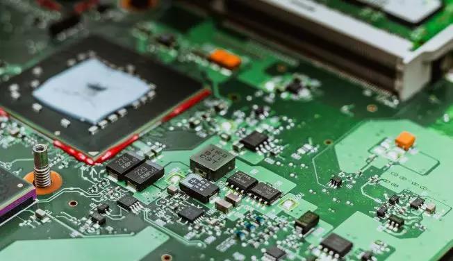


Just upload Gerber files, BOM files and design files, and the KINGFORD team will provide a complete quotation within 24h.