
Professional PCB manufacturing and assembly
Building 6, Zone 3, Yuekang Road,Bao'an District, Shenzhen, China
+86-13410863085Mon.-Sat.08:00-20:00

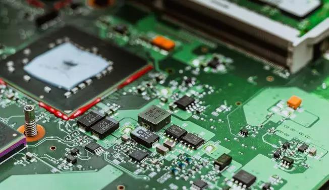
PCB design component layout principles
1. The components should be designed inside the PCB board, and each outlet foot of the components should occupy a separate pad.
2, components can not occupy the entire PCB panel, the board around to leave a margin of 5~10mm, and the size of the PCB board area and fixed way determines the size of the margin around the board.
3. Components are required to be evenly distributed and uniformly spaced on the entire layout.
4. The installation height of components should be as low as possible. If it is too high, it is easy to fall or collide with adjacent components, so it may lead to poor safety performance of the system.
5, to determine the axial position of the larger components is the installation state of the printed circuit board in the system, the axis direction of the regular arrangement of components should be in the vertical direction of the system, so as to improve the stability of components on the printed circuit board.
6. The span at both ends of the components should be slightly larger than the axial length of the components. When bending the pin, do not bend at the root. Leave a distance of about 2mm to avoid damaging the components.
7. The layout of components cannot be crossed up and down, and a certain distance should be maintained between adjacent components and the spacing should not be too small.
For capacitor installation, the first thing to mention is the installation distance. The capacitor with the smallest capacity has the highest resonant frequency and the smallest decoupling radius, and is therefore placed closest to the chip. The one with the larger capacity can be a little farther away, and the outermost one with the largest capacity. However, all capacitors decoupled from the chip are kept as close to the chip as possible.
Another point to note is that when placed, it is best to distribute evenly around the chip for each capacity level. Usually the design of the chip takes into account the arrangement of power and ground pins, which are generally evenly distributed on the four sides of the chip. Therefore, voltage perturbations exist all around the chip, and decoupling must also be evenly decoupled across the entire chip region. Capacitors are placed at the top of the chip, and because of the decoupling radius problem, the voltage perturbations below the chip cannot be decoupled well.
Installation of capacitance
When installing the capacitor, pull out a small length of lead wire from the pad, and then connect it to the power plane through the hole, as well as the ground end. In this way, the current loop flowing through the capacitor is as follows:Power plane -- through hole -- lead wire -- pad -- capacitor -- pad -- lead wire -- through hole -- ground plane.

The first method leads a long lead from the pad and then connects through the hole, which will introduce a large parasitic inductance, must avoid doing this, this is the worst installation way.
The second method is to drill holes in the two ends of the pad next to the pad, which is much smaller than the first method, and the parasitic inductance is also smaller, which can withstand.
The third in the side of the pad drilling, further reduce the loop area, parasitic inductance is smaller than the second, is a better method.
The fourth is drilled on both sides of the pad. Compared with the third method, each end of the capacitor is connected to the power plane and the ground plane in parallel through the hole, which is smaller than the third parasitic inductance, only space allows, as far as possible with this method.
The last method is to punch holes directly on the pad, the parasitic inductance is minimal, but welding is likely to cause problems, whether to use depends on the processing ability and way.
Recommend using the third and fourth methods.
It is important to note that some engineers use common holes for multiple capacitors on the circuit board to save space. Do not do this under any circumstances. It is best to find ways to optimize the design of the capacitor combination and reduce the number of capacitors.
Because the wider the printed line, the smaller the inductance, the lead line from the pad to the hole should be widened as far as possible, and the width of the pad should be the same. This allows you to use 20mil wide leads, even for 0402 capacitors.

Eight PCB panel guide
Jan 31,2023


Just upload Gerber files, BOM files and design files, and the KINGFORD team will provide a complete quotation within 24h.