
Professional PCB manufacturing and assembly
Building 6, Zone 3, Yuekang Road,Bao'an District, Shenzhen, China
+86-13410863085Mon.-Sat.08:00-20:00

How pcb designers choose appropriate pcb design tools to share
The following are some factors that PCB designers must consider and will influence their decisions:
1. Product Functions
A. The basic functions of the basic requirements of the cover include:
a. Interaction between schematic diagram and PCB layout
b. Automatic fanout routing, push-pull and other routing functions, as well as routing capability based on design rule constraints
c. Precise DRC verifier
B. The ability to upgrade product functions when the company is engaged in a more complex design
a. HDI (High Density Interconnect) interface
b. Flexible design
c. Embedded passive components
e. Automatic script is born
f. Topology Layout Routing
g. DFF, DFT, DFM, etc
C. Additional products can perform analog simulation, digital simulation, analog digital mixed signal simulation, high-speed signal simulation and RF simulation
D. Have a central component library that is easy to create and manage
2. A good partner who is technically in the industry leadership and has devoted more efforts than other manufacturers can help you design products with the greatest efficiency and leading technology in the shortest time
3. Price should be the most secondary factor among the above factors, and more attention should be paid to the return on investment!
PCB evaluation needs to consider many factors. The type of development tools designers are looking for depends on the complexity of the design work they are engaged in. Because the system is becoming more and more complex, the control of physical routing and electrical component placement has developed to a very wide extent, so that it is necessary to set constraints for the hub path in the design process. However, too many design constraints constrain the flexibility of design. Designers must have a good understanding of their design and its rules, so that they can clearly understand when to use these rules.
It shows a typical front to back integrated system design. It starts with a design definition (schematic input), which is closely integrated with constraint compilation. In constraint compilation, designers can define both physical and electrical constraints. Electrical constraints will drive the simulator for pre layout and post layout analysis for network validation. Take a closer look at the design definition, which is also linked to FPGA/PCB integration. The purpose of FPGA/PCB integration is to provide bidirectional integration, data governance and the ability to perform collaborative design between FPGA and PCB.
In the layout phase, the same constraint rules for physical implementation as in the design definition phase are entered. This reduces the probability of making mistakes from the file to the layout. Pin exchange, logic gate exchange, and even input/output interface group (IO_Bank) exchange all need to return to the design definition stage for updating, so the design of each phase is synchronized.
During the evaluation, designers must ask themselves: What scale is important to them?
Let's take a look at some trends that force designers to review their existing development tool capabilities and start ordering new ones:
1. RF design
For RF design, RF circuit should be directly designed into system schematic diagram and system board layout, rather than a separate environment for subsequent conversion. All simulation, tuning and optimization capabilities of the RF simulation environment are still necessary, but the simulation environment can accept more original data than the "actual" design. Therefore, the differences between data models and the problems of design transformation caused by them will disappear. First, designers can directly interact between system design and RF simulation; Secondly, if designers carry out a large-scale or reasonably complex RF design, they may want to assign circuit simulation tasks to multiple computing platforms running in parallel, or they may want to send each circuit in a design composed of multiple modules to their respective simulators to shorten the simulation time.
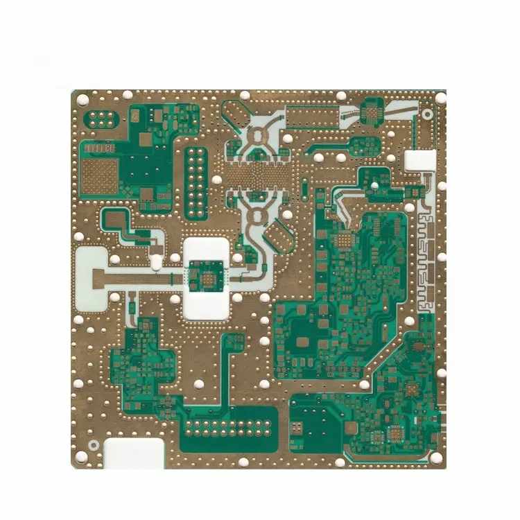
2.HDI
The increase of semiconductor complexity and the total number of logic gates has required more pins and finer pin spacing for integrated circuits. It is very common to design more than 2000 pins on a BGA device with a pin spacing of 1mm, let alone to arrange 296 pins on a device with a pin spacing of 0.65mm. The need for faster rise times and signal integrity (SI) requires more power and ground pins, which requires more layers in the multilayer board, thus driving the need for high-density interconnection (HDI) technology for micro vias.
HDI is an interconnection technology being developed in response to the above needs. Micro vias and ultra-thin dielectrics, thinner routing and smaller line spacing are the main features of HDI technology.
In order to design a rigid flexible PCB, all factors that affect the assembly process must be considered. The designer cannot simply design a rigid flexible PCB as if it were another rigid PCB. They must manage the bending area of the design to ensure that the design point will not cause the conductor to break and peel due to the stress action of the bending surface. There are still many mechanical factors to consider, such as minimum bending radius, dielectric thickness and type, sheet metal weight, copper plating, overall circuit thickness, number of layers, and number of bending sections.
Understand rigid flexible design and decide whether your product will allow you to create a rigid flexible design.
4. Packaging
The increasing functional complexity of modern products requires a corresponding increase in the number of passive components, mainly reflected in the increase in the number of decoupling capacitors and terminal matching resistors in low power and high-frequency applications. Although the package of passive surface mount devices has shrunk considerably after several years, the results are still the same when trying to obtain the maximum limit density. Printed component technology has transformed from multi chip module (MCM) and hybrid module to SiP and PCB that can be directly used as embedded passive components today. In the process of transformation, the latest assembly technology was adopted. For example, including an impedance material layer in a layered structure and using a series terminal resistor directly under the uBGA package have greatly improved the function of the circuit. Now, embedded passive components can obtain high-precision design, thus eliminating the additional processing steps of laser cleaning welds. Wireless components are also developing towards the direction of improving integration directly in the substrate.
5. Signal integrity planning
In recent years, new technologies related to parallel bus structure and differential pair structure for serial parallel transformation or serial interconnection have been continuously improved. The type of typical design problems encountered in a parallel bus and serial parallel conversion design. The limitation of parallel bus design lies in the change of system timing, such as clock skew and propagation delay. Because of clock skew in the whole bus width, the design of timing constraints is still difficult. Increasing the clock speed will only make the problem worse.
On the other hand, the differential pair architecture uses a swappable point-to-point connection at the hardware level to achieve serial communication. Usually, it transfers data through a one-way serial "channel", which can be stacked into 1 -, 2 -, 4 -, 8 -, 16 - and 32 width configurations. Each channel carries one byte of data, so the bus can handle data width from 8 bytes to 256 bytes, and can maintain data integrity by using some forms of error detection techniques. However, because of the high data rate, other design problems arise. The clock recovery in high frequency becomes the burden of the system. Because the clock needs to quickly lock the input data stream, and to improve the circuit's anti shake function, it is also necessary to reduce the jitter between all cycles. Power noise also poses additional problems for designers. This type of noise increases the possibility of severe jitter, which will make eye opening more difficult. Another challenge is to reduce common mode noise and solve problems caused by loss effects from IC packages, PCB boards, cables and connectors.
It seems that it is easy to obtain a PCB tool that can handle the layout; But it is crucial to obtain a tool that can not only satisfy the layout but also solve your urgent needs.


Just upload Gerber files, BOM files and design files, and the KINGFORD team will provide a complete quotation within 24h.