
Professional PCB manufacturing and assembly
Building 6, Zone 3, Yuekang Road,Bao'an District, Shenzhen, China
+86-13410863085Mon.-Sat.08:00-20:00

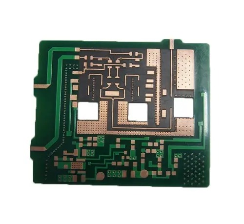
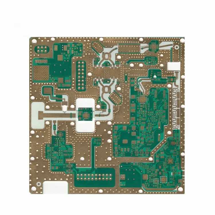
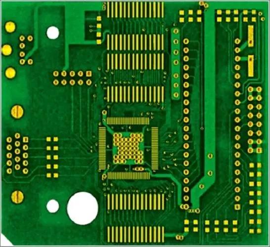
PCB Vocabulary Commonly Used by MI Engineers in PCB Design
PCB vocabulary commonly used by MI engineers for explaining PCB design by PCB assembly and PCB processing manufacturers.
1. OSP: Organic Solvency Protector;
2. BGA: Ball Grid Array: the packaging form of integrated circuit, whose input and output points are tin balls arranged in grid style on the bottom surface of components;
3. Blind via: the conductive connection between the outer layer and the inner layer of a PCB does not continue to the other side of the board; Buried via: conductive connection between two or more inner layers of a PCB (i.e. invisible from the outer layer);
4. Material Thickness (Board Thickness): if there is no special description in the customer's drawings or specs, it refers to the finished thickness. If there is no tolerance requirement for Material Thickness, the closest thickness shall be selected;
5. Warp and Fill: Warp refers to the short direction of large material (or Prepreg), and Fill refers to the long direction of large material (or Prepreg).
6. Horizontal material and straight material: when the multilayer board is cut, the long direction of the panel is consistent with the long direction of the large material; The panel whose long direction is consistent with the short direction of the large material is called the horizontal material;
7. Copper Thickness: refers to the thickness of finished line copper unless otherwise specified in the customer's drawings or specs;
8. Pitch: pitch, the distance between adjacent conductor centers;
9. Solder Mask Clearance: diameter of green window;
10. LPI solder mask oil: Liquid Photo Imaging solder mask oil, commonly known as wet green oil;
11. SMOBC: Solder Mask On Bare Copper green silk screen printed on the polished copper surface, generally including SMOBC+HAL/Entek/ENIG and other processes;
12. Lead Free: Lead-Free;
13. Halogen Free: Halogen free, ring shaped material;
14. RoHS: Restriction of Use of Hazardous Substances, prohibition of lead, mercury, Cadmium, Hexavalent Chromium and Flame Retardents;
15CTI: Comparative Tracking Index, that is, the maximum voltage value at which the material surface can withstand 50 drops of electrolyte without forming a leakage trace;
16. PTI: Proof Tracking Index, that is, the withstand voltage value of the material surface that can withstand 50 drops of electrolyte without forming leakage marks is expressed in V;
17. Tg: Glass Transition temperature;
18. Hole test paper: drawings printed out in 1:1 for each test point and pipe position;
19. Test points: generally refer to independent PTH holes, SMT PADs, gold fingers, bonding fingers, IC fingers, BGA welding points, and test points tested by customers after plug-ins;
20. Test endpoint: the test point in the line network that cannot be extended forward.
21. Positive Pattern: the figure when the conductive figure on the positive image, positive film, photographic original and production plate is opaque;
22. Negative Pattern: Negative image pattern, negative film, the conductive pattern on the original photographic plate and production plate is transparent. We generally call direct etching line film, green oil blocking ink film and dry/UV green oil film as negative film; The required electroplated line film, wet green oil film, character film, carbon oil film and blue gel film are called positive film;
23. FPT: Fine Pitch Technology, the distance between leading angle centers of SMT component packaging is 0.025 "(0.0635mm) or less. PCB terms commonly used by MI engineers who explain PCB design by PCB assembly and PCB processing manufacturers.


Just upload Gerber files, BOM files and design files, and the KINGFORD team will provide a complete quotation within 24h.