
Professional PCB manufacturing and assembly
Building 6, Zone 3, Yuekang Road,Bao'an District, Shenzhen, China
+86-13410863085Mon.-Sat.08:00-20:00

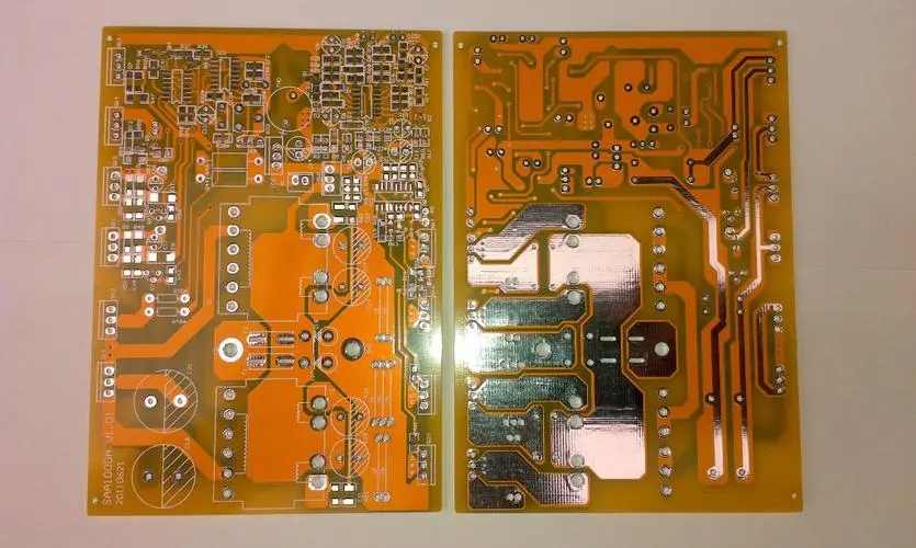
Hardware layout experience of circuit board design in electronic factory
The circuit board manufacturer explains the clock wiring, interface wiring and board stacking of circuit board hardware design.
Clock cable routing
1. No clock wiring on the surface layer or wiring length=<500mil (key clock surface wiring=<200mil); In addition, the complete ground plane shall be used as the return current, and the undivided or separated positions shall be bridged.
2. No other wiring passes through the TOP layer in the crystal oscillator and clock drive circuit area; (This is sometimes difficult to satisfy.).
3. Other signal lines shall be avoided around the signal lines, and the 3W principle shall be met when necessary (the center distance between the two lines shall be 3 times of the line width). This is generally not considered when arranging data lines or address lines, but the timing (equal length) is emphasized.
4. If possible, the power supply layer should meet the 20h principle as far as possible: that is, the boundary of the power supply layer is 20 times the thickness of the shrinkage plate inside the stratum boundary.
**20H rule: because the electric field between the power layer and the stratum is variable, electromagnetic interference will be radiated at the edge of the board. It is called edge effect. The power layer can be shrunk in such a way that the electric field is only conducted within the range of the ground plane. In the unit of one H (the thickness of the medium between the power supply and the ground), 70% of the electric field can be limited to the grounding edge if it is reduced by 20H; Shrinking 100H can limit 98% of the electric field.
5. The clocks of different frequencies meet the 3W principle
**3W rule: In order to reduce the interference between lines, ensure that the line spacing is large enough. When the line center distance is not less than 3 times the line width, 70% of the electric fields can not interfere with each other, which is called 3W rule. If 98% of the electric fields do not interfere with each other, the 10W rule can be used.
6. When the clock signal layer is changed and the return reference plane is also changed, a grounding hole is generally arranged next to the clock wire layer change hole.
7. The distance between clock wiring and I/O interface, handle bar is>=1000 mil.
8. The equal length of clock line and adjacent plane layer wiring is<=1000 mil.
9. The multi load clock structure shall be star shaped as far as possible. In practical implementation, it is generally adopted to carry out equal length bifurcation when walking to the relative center of the multi load point.
10. In SDRAM cabling, the length difference between SDCLK and DATA is<=800mil.
11. The typical transmission speed of stripline (middle layer routing) is 180ps/inch, and that of microstrip line (surface layer routing) is 140ps/inch.
Interface wiring requirements:
1. Difference distribution line rules: parallel and equidistant, same layer, equal length.
2. The network length between interface transformer and interface connector is less than 1000ml.
3. Bridging measures shall be taken for the reset line across the division.
4. The wiring of interface circuit shall follow the principle of protection before filtering.
5. The primary and secondary isolation devices such as interface transformer and optocoupler are isolated from each other, without coupling paths such as adjacent planes, and the isolation width of corresponding reference planes is greater than 100mil.
Stacking of plates:
1. The adjacent layer of the element layer is the ground plane, which provides the device shielding layer and the reference plane for the fixed layer wiring layer.
2. All signal layers shall be adjacent to the ground plane as much as possible.
3. Try to avoid two signal layers being directly adjacent.
4. The main power supply shall be adjacent to its corresponding ground as far as possible.
5. Take into account the symmetry of laminated structure.
Other wiring precautions:
1. The EMC environment between the power supply layer and the stratum is poor, so the signal sensitive to interference should be avoided.
2. The signal line must have no right angle.
3. The wiring shall be close to one plane as far as possible, and cross division shall be avoided. If it is necessary to cross division or cannot be close to the power ground plane, these conditions are only allowed to exist in low-speed signal lines. The circuit board assembly, circuit board design, and circuit board processing manufacturers explain the hardware layout experience of the circuit board design of the electronics factory.


Just upload Gerber files, BOM files and design files, and the KINGFORD team will provide a complete quotation within 24h.