
Professional PCB manufacturing and assembly
Building 6, Zone 3, Yuekang Road,Bao'an District, Shenzhen, China
+86-13410863085Mon.-Sat.08:00-20:00

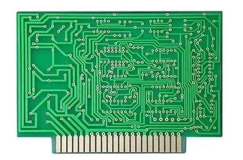
PCB Design of Smart Phone in PCB Factory - Introduction to Shielding Cover
The shield cover/case/basket is an alloy metal cover, which is an important part to reduce the radiation of the display. Inside the display are electronic guns, high-voltage packages, circuit boards and other components, which emit high intensity electromagnetic radiation when working. The shielding cover can play a role of shielding, blocking some of the electromagnetic waves in the cover, so as to protect users from the harm of electromagnetic radiation, while avoiding interference to other electrical appliances around, to a certain extent, it also ensures that the components are free from dust, and extends the service life of the display. It is mainly used in mobile phones, GPS and other fields.
Shielding is the metal isolation between two space areas to control the induction and radiation of electric field, magnetic field and electromagnetic wave from one area to another. Specifically, shielding is used to enclose interference sources of components, circuits, assemblies, cables or the whole system to prevent interference electromagnetic fields from spreading outwards; Enclose the receiving circuit, equipment or system with shielding to prevent them from being affected by external electromagnetic fields. Because the shield can absorb energy (eddy current loss), reflect energy (interface reflection of electromagnetic wave on the shield) and counteract energy (electromagnetic induction generates reverse electromagnetic field on the shield layer, which can counteract part of the interference electromagnetic wave) to the external interference electromagnetic wave and internal electromagnetic wave from wires, cables, components, circuits or systems, etc. Circuit board assembly, circuit board design, and circuit board processing manufacturers explain the design of smart phone PCB shield,
(1) When the frequency of the interference electromagnetic field is high, the eddy current generated in the metal material with low resistivity is used to counteract the external electromagnetic wave, so as to achieve the shielding effect.
(2) When the frequency of interference electromagnetic wave is low, materials with high permeability shall be used, so as to limit the magnetic line of force inside the shielding body and prevent it from spreading to the shielding space.
(3) In some cases, if high frequency and low frequency electromagnetic fields are required to have a good shielding effect, different metal materials are often used to form a multi-layer shield.
1. The cover material can be ZSNH zinc tin nickel alloy (cheap), white copper (good performance and easy processing), or stainless steel (can only be used as the cover without tin). The support material shall be ZSNH zinc tin nickel alloy or white copper to ensure good welding performance. But now some customers have used ZSNH to make the upper and lower covers.
2. The thickness of ZSNH zinc tin nickel alloy base is 0.2mm, and the cover is 0.13mm. Stainless steel cover 0.13mm ocean white copper base thickness 0.2mm, cover 0.13mm, single piece, two-piece, material: ocean white copper, stainless steel, ZSNH zinc tin nickel alloy
3. The clearance around the cover and bracket is 0.05mm, the z-direction clearance is 0mm, and the distance from the components is more than 0.4mm
4. After flattening, the width of the punching area shall be 0.5mm.
5. The width of the shield cover pad is 0.7mm~1mm, which is too small for mounting and too large for external interference. The minimum clearance between the shield cover and the bottom of the shield cover shall be 0.5mm (the minimum clearance between the support pad and the pad shall also be 0.3mm).
6. When the support is smt, the floating tin height is 0.1mm, and the flatness of the cover is 0.1mm. The minimum clearance between the shield cover and the device or shell above shall be 0.2mm after assembly
7. The suction cup area with a diameter of 5mm shall be pre designed at the center of gravity of the shielding support.
8. One or two through holes with a diameter of 0.7~1mm shall be provided on each side of the wall around the shielding support to clamp the shielding cover. There should not be too many holes, otherwise it is difficult to disassemble, which can be made by the supplier. We will give the location and size.
9. The bottom of the walls around the shield cover should be 0.5mm away from the PCB to prevent the shield bracket from eating too much tin to support the shield cover.
10. The diameter of the heat dissipation hole of the shield cover is 1mm.
11. If the shield cover or shield support has a plane drop, pay attention to the side cut through at the drop boundary, otherwise it cannot be processed. In addition, holes with a diameter of 3mm shall be drilled at the drop corners in the plane, otherwise they will tear.
12. If the shield cover or shield support has a plane drop, pay attention to the drop angle of 35~40 degrees. If the angle is too large, it will be cracked during processing.
13. If the shield cover or shield support has a plane drop, the fit clearance between the support and the cover surface at the drop is not 0, which should be 0.1mm.
14. The distance between the plane cutout of the shielding support and the outer wall of the side wall shall be more than 1mm. If there is a downward bend inside, the side wall at the bend shall be 0.5mm away from the outer wall. At this time, the plane is directly adjacent to the side wall cutout.
15. Inner angle of shielding support clearance area is R0.5mm.
16. The shield bracket and PCB are not welded on the whole surface. The 2-1-2-1mm Great Wall foot shall be used for welding, with 2mm contact and 1mm suspension for easy tin climbing. This can increase the adhesion strength of the shield cover.
17.1. It is made with SHIEDING-BOX.
2. The surface flatness is within 0.1MM.
3. The bending internal angle is R0.1MM, and the unmarked fillet is R0.1MM.
4. The bending angle is 90 °± 0.5.
5. Undeclared tolerance shall be in accordance with the tolerance grade shown in the drawing
6. The dimensions marked with "*" in the drawing are QC controlled dimensions.
7. Please check with the engineer before opening the mold. (Tolerance dimension: the dimension smaller than 20mm shall be controlled at+-0.05mm; the dimension larger than 20mm shall be controlled at+-0.1mm; the top floor flatness shall be controlled at+-0.1mm;) Circuit board assembly, circuit board design, and circuit board processing manufacturers explain the design of smart phone PCB shield.


Just upload Gerber files, BOM files and design files, and the KINGFORD team will provide a complete quotation within 24h.