
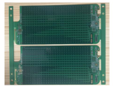
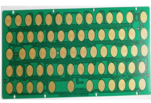
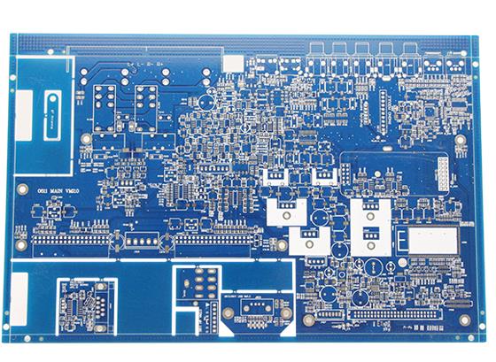
Professional PCB manufacturing and assembly
Building 6, Zone 3, Yuekang Road,Bao'an District, Shenzhen, China
+86-13410863085Mon.-Sat.08:00-20:00

Eight safety distances must be considered in PCB design
PCB manufacturers, PCB designers and PCBA manufacturers will explain the eight safety distances that PCB manufacturers must consider in PCB design
In PCB factory design, there are many places that need to consider safe spacing, including wire spacing, character spacing, pad spacing, etc. Here, it is temporarily classified into two categories: one is electrical related safety spacing, and the other is non electrical related safety spacing.
01 Electrical related safety distance
1. Spacing between conductors
As far as the processing capacity of mainstream PCB manufacturers is concerned, the minimum distance between conductors shall not be less than 0.075mm. Minimum line distance refers to the minimum distance between board sub line and line, and between line and pad. From the production point of view, the larger the line spacing is, the better. The common one is 0.25mm.
2. Pad aperture and pad width
As far as the processing capability of mainstream PCB manufacturers is concerned, if the pad is mechanically drilled, the minimum hole diameter shall not be less than 0.2mm; In case of laser drilling, the minimum hole diameter shall not be less than 0.1mm.
The hole diameter tolerance is slightly different according to different plates, which can be controlled within 0.05mm generally, and the minimum pad width shall not be less than 0.2mm.
3. Spacing between pads
As far as the processing capability of mainstream PCB manufacturers is concerned, the spacing between pads shall not be less than 0.2mm.
4. Spacing between copper sheet and plate edge
The distance between the live copper sheet and the PCB edge should be no less than 0.3mm. You can set this spacing rule on the Design Rules Board outline page.
In case of large-area copper laying, there is usually a contraction distance with the plate edge, which is generally set as 0.5mm. In PCB design and manufacturing industry, in general, due to the mechanical considerations of the finished circuit board, or to avoid the possibility of curling or electrical short circuit due to the exposure of the copper sheet on the board edge, engineers often shrink the large area of copper block with respect to the board edge by 20 mils, instead of always laying the copper sheet to the board edge.
There are many methods to deal with the copper skin shrinkage, such as drawing a keepout layer on the board edge, and then setting the distance between copper and keepout. A simple method is introduced here, which is to set different safety distances for the copper laying objects. For example, if the safety distance of the whole board is set to 0.25mm, and the copper laying is set to 0.5mm, the board edge can be shrunk by 0.5mm. At the same time, the possible dead copper in the device can be removed.
02 Non electrical related safety distance
1. Character width, height and spacing
The PCB factory cannot make any changes during the text film processing, but only thicken the character line width below D-CODE 0.22mm (8.66mil) to 0.22mm, that is, the character line width L=0.22mm (8.66mil).
The width of the whole character W=1.0mm, the height of the whole character H=1.2mm, and the spacing between characters D=0.2mm. When the text is less than the above standard, it will be blurred after processing and printing.
2. Clearance between vias
The distance between vias (VIA) and vias (hole edge to hole edge) should be better than 8mil.
3. Distance from silk screen to pad
The PCB manufacturer requires that the screen printing is not allowed to cover the bonding pad. Because if the solder pad is covered with the silk screen, the silk screen cannot be coated with tin, which affects the assembly of components. Generally, it is better to reserve a space of 8mil for the plate factory. If the area of PCB board is limited, the spacing of 4mil is barely acceptable. If the silk screen accidentally covers the bonding pad during design, the plate factory will automatically eliminate the silk screen left on the bonding pad during manufacturing to ensure tin on the bonding pad.
Of course, the specific situation shall be analyzed in the design. Sometimes the silk screen is deliberately close to the bonding pad, because when two bonding pads are close together, the middle silk screen can effectively prevent short circuit of solder connection during welding, which is another case.
4. 3D height and horizontal spacing on machinery
When assembling and pasting PCB factory components, it is necessary to consider whether the horizontal direction and space height will conflict with other mechanical structures. Therefore, in the design, it is necessary to fully consider the adaptability between components, between PCB finished products and product shells, and on the spatial structure, and reserve a safe space for each target object to ensure that there is no conflict in space. PCB manufacturers, PCB designers and PCBA manufacturers will explain the eight safety distances that PCB manufacturers must consider in PCB design


Just upload Gerber files, BOM files and design files, and the KINGFORD team will provide a complete quotation within 24h.