
Professional PCB manufacturing and assembly
Building 6, Zone 3, Yuekang Road,Bao'an District, Shenzhen, China
+86-13410863085Mon.-Sat.08:00-20:00

Wiring arrangement and reasonable layout of components on PCB
PCB manufacturers, PCB designers and PCBA manufacturers explain the wiring arrangement and reasonable layout of components on PCB
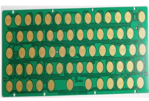
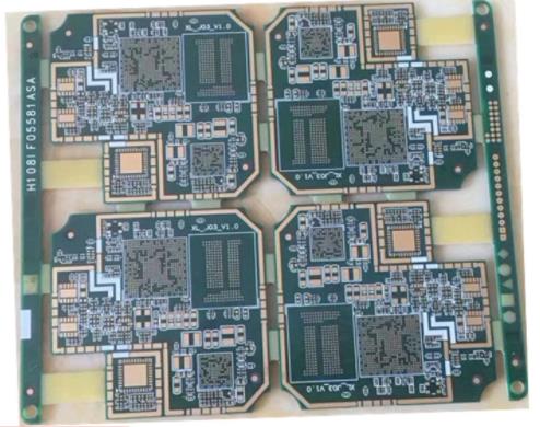
Printed circuit boards, also known as printed circuit boards, are providers of electrical connections for electronic components.
Printed circuit board is usually represented by "PCB", not "PCB".
PCB design is mainly layout design; The main advantage of using circuit board is to greatly reduce wiring and assembly errors, and improve the automation level and production labor rate.
(1) No cross circuit is allowed in the printed circuit board. The possible cross lines can be solved by "drilling" or "winding". That is to say, let a lead "drill" through the gap at the foot of other resistors, capacitors, and transistors, or "wind" through one end of a lead that may cross. Under special circumstances, how to make the circuit very complex? In order to simplify the design, it is also allowed to use a wire jumper to solve the cross circuit problem.
(2) Resistance, diode, tubular capacitor and other components can be installed in "vertical" and "horizontal" modes. Vertical refers to the installation and welding of components perpendicular to the circuit board, which has the advantage of saving space. Horizontal refers to the installation and welding of components parallel to and close to the circuit board, which has the advantage of good mechanical strength for component installation. For these two different mounting components, the component hole spacing on the printed circuit board is different.
(3) The grounding point of the circuit at the same level shall be as close as possible, and the power filter capacitor of the circuit at this level shall also be connected to the grounding point at this level. In particular, the grounding points of the base and emitter of the current transistor cannot be too far away, otherwise the copper foil between the two grounding points is too long, which will cause interference and self excitation. The circuit using this "one point grounding method" works stably and is not easy to self excitation.
(4) The general grounding wire must be arranged in the order from weak current to strong current in a high frequency medium frequency low frequency level. It is not allowed to randomly turn over and over. It is better to have a long connection between levels, but also to comply with this provision. In particular, the grounding wire arrangement of frequency converter head, regeneration head and frequency converter head is more strict. If it is improper, self excitation will occur and it will not work.
High frequency circuits such as FM head often use a large area of enclosed ground wire to ensure a good shielding effect.
(5) Strong current leads (common ground wire, power amplifier power lead, etc.) should be as wide as possible to reduce wiring resistance and its voltage drop, and reduce self excitation caused by parasitic coupling.
(6) The route with high impedance shall be as short as possible, and the route with low impedance may be longer, because the route with high impedance is easy to whistle and absorb signals, causing circuit instability. The power line, ground wire, base wire without feedback component, emitter wire, etc. are all low impedance wires. The base wire of the emitter follower and the ground wire of the two audio channels of the radio recorder must be separated and formed into one circuit respectively until the end of the function. If the two ground wires are connected, it is very easy to produce crosstalk and reduce the separation.
PCB manufacturers, PCB designers and PCBA manufacturers will explain the wiring arrangement and reasonable layout of components on PCB.


Just upload Gerber files, BOM files and design files, and the KINGFORD team will provide a complete quotation within 24h.