
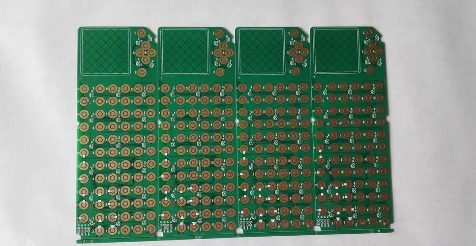
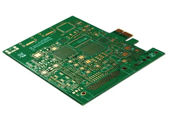
Professional PCB manufacturing and assembly
Building 6, Zone 3, Yuekang Road,Bao'an District, Shenzhen, China
+86-13410863085Mon.-Sat.08:00-20:00

Pcb proofing high-speed digital system physical rule driving and electrical rule driving
In general, when the signal interconnection delay is greater than 20% of the edge signal turnover threshold time, the signal wire on the board will show the transmission line effect, that is, the wire is no longer a simple wire performance that shows the lumped parameters, but a distributed parameter effect. This design is a high-speed design. In the design of high-speed digital systems, the designer must solve the problems of false switching and signal distortion caused by parasitic parameters - real-time sequence and signal integrity. At present, this is also a bottleneck problem that high-speed circuit designers must solve.
Traditional physical rule driven pcb proofing
We can find that in the traditional high-speed circuit design, electrical rule setting and physical rule setting are separated. This brings about the following defects:
In the early stage of design, engineers have to spend a lot of energy on detailed front-end and back-end (i.e., logical establishment physical implementation) analysis to plan a physical cabling strategy to meet electrical requirements.
High speed effect is a complex subject, which can not be achieved by simply controlling the length of wiring and parallel lines.
The designer will inevitably face such a dilemma that the physical rules with false elements are not applicable in the actual wiring, and he has to modify the rules repeatedly to make them practical.
After the wiring is completed, the post validation tool can be used for analysis. However, if problems are found, engineers must return to the design and adjust the structure or rules. This is a cyclic redundant process. It will inevitably affect the time to market.
When there are only a few or dozens of key networks in the design, physical rule driven can well complete the design task; But when there are hundreds or even thousands of wire networks in the design, the physical rule driven method is not competent for the design task at all. The development of electronic technology calls for new methods and tools to solve the bottleneck problems faced by design. In order to solve the defects of physical rule driven high-speed design, the industry's knowledgeable people engaged in the research and development of high-speed digital circuit design EDA tools proposed the concept of real-time electrical rule driven physical layout and routing three years ago, and reformed the high-speed digital design process from the design idea.
A new electric rule driven pcb proofing: interconnection synthesis
Interconnection synthesis is a typical term of real-time electrical rule driven method, that is, in the process of physical layout and routing, the interconnection synthesizer analyzes in real time according to the constraints of electrical rules, extracts the routing strategies that meet the requirements of the designer, and makes the design successful at one time. This method integrates electrical requirements and physical realization accurately through interconnection synthesis, and fundamentally eliminates the defects of physical rule driven method.
The integrated process of pcb proofing interconnection is as follows:
Input noise constraint and time order constraint rules in the tool;
Timing control layout to meet timing constraints;
Perform signal integrity pre optimization;
Board level integration to ensure that the key line network meets the electrical requirements;
Complete the wiring of ordinary wire network;
Comprehensive optimization of cabling.
The electrical rule driven method can effectively evaluate the quality before designing the layout and routing, detect the signal distortion, and determine the matching network topology and appropriate terminal matching structure and resistance value. After the layout and wiring is completed, post verification can be carried out, and the waveform can be intuitively detected with the software oscilloscope. The timing and distortion problems found at this time can be solved by the routing comprehensive optimization function.
PCB manufacturers, PCB designers and PCBA manufacturers will explain the physical rule drive and electrical rule drive of the high-speed digital system for pcb proofing.


Just upload Gerber files, BOM files and design files, and the KINGFORD team will provide a complete quotation within 24h.