
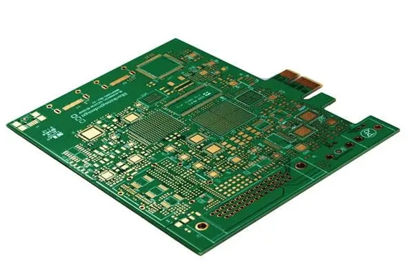
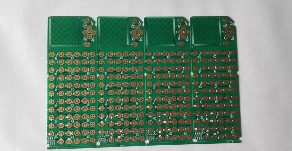
Professional PCB manufacturing and assembly
Building 6, Zone 3, Yuekang Road,Bao'an District, Shenzhen, China
+86-13410863085Mon.-Sat.08:00-20:00

Pcb proofing gold tool combination, mixed signal, traditional serial design
Now many EDA manufacturers can provide EDA tools for high-speed system PCB design to help users effectively improve design quality and shorten design cycle in this field. Among EDA system board level tools that apply electric rule driven method, the most representative is MentorGraphics ICX software package. It was the first to put forward the concept of interconnection integration, and it is also the most mature tool combination in the industry. This software package has the characteristics of plug and play, which is popular in the industry at present. It can be integrated in the classic EDA design process of PCB of many manufacturers.
Mixed signal design solution for pcb proofing
As the miniaturization of design has become fashionable, consumers need high-performance and low-cost goods. In order to adapt to market competition, manufacturers require R&D personnel to develop high-performance and low-cost products of different types and functional configurations in the shortest possible time to occupy the market. This brings designers many new design challenges. For example, using digital analog mixed technology, or even RF technology on the same substrate, to achieve the purpose of miniaturization of design and improvement of product functions. The mobile phone that is popular all over the world is a typical example. The industry also has corresponding solutions - design team, concurrent design, derivation and design reuse are the most typical strategies.
Traditional serial design of pcb proofing
That is, after the electronic engineer completes all the front-end circuit design, he will transfer it to the physical board level designer to complete the back-end implementation. The design cycle is the sum of circuit design and board level design time. After the miniaturization has become the mainstream design idea and the hybrid technology has been widely adopted, the serial design method has fallen behind. We must innovate in design methods and use powerful EDA tools to assist designers in design, so as to meet the requirements of timely listing. As we all know, it is impossible for each of us to become an expert in all fields, and it is impossible to complete all the work best and fastest in a short time. The concept of design team was put forward in this context and has been widely applied. At present, many companies adopt the method of design team to cooperate in product development. That is, according to the complexity of the design and different functional modules, the whole design is divided into different functional BLOCK blocks, and different designers and developers design logic circuits and PCB boards in parallel; Then, at the top level of the design, the final design results of each BLOCK block are called in as "devices" to form a whole board design. This method is called PCB design reuse. Through this method, we can see that it can greatly shorten the design cycle. The design time is only the sum of the design time of the BLOCK block that takes the most time and the time of the back-end interface connection processing.


Just upload Gerber files, BOM files and design files, and the KINGFORD team will provide a complete quotation within 24h.