
Professional PCB manufacturing and assembly
Building 6, Zone 3, Yuekang Road,Bao'an District, Shenzhen, China
+86-13410863085Mon.-Sat.08:00-20:00

1. PCB wiring and layout isolation criteria: strong and weak current isolation, large and small voltage isolation, high and low frequency isolation, input and output isolation. The dividing standard is an order of magnitude difference. The isolation methods include space separation and ground wire separation.
2. The crystal oscillator should be as close to the IC as possible, and the wiring should be thick
3. Crystal case grounding
4. When the clock wiring is output through the connector, the contact pin on the connector shall be covered with grounding contact pin around the clock wire contact pin
5. Let analog and digital circuits have their own power supply and ground wire paths. If possible, widen the power supply and ground wire of these two parts of circuits or use separate power supply and ground layers to reduce the impedance of power supply and ground wire circuits and reduce any possible interference voltage in power supply and ground wire circuits
6. The analog ground and digital ground of the PCB working independently can be connected together at a single point near the system grounding point. If the power supply voltage is consistent, the power supplies of the analog and digital circuits can be connected together at a single point at the power supply inlet. If the power supply voltage is inconsistent, a 1~2nf capacitor will be added near the two power supplies to provide a path for the signal return current between the two power supplies
7. If the PCB is inserted on the motherboard, the power and ground of the analog and digital circuits of the motherboard should also be separated. The analog ground and digital ground should be grounded at the motherboard ground, and the power supply should be connected at a single point near the system ground point. If the power supply voltage is consistent, the power supply of the analog and digital circuits should be connected at a single point at the power source inlet. If the power supply voltage is inconsistent, a 1~2nf capacitor should be connected near the two power supplies to provide a path for the signal return current between the two power supplies
8. When high-speed, medium speed and low-speed digital circuits are mixed, they should be assigned different layout areas on the printed board
9. Separate low-level analog circuit and digital logic circuit as much as possible
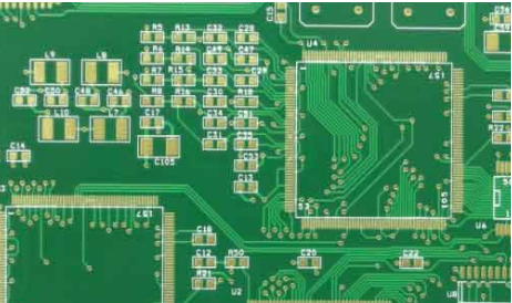
10. When designing multilayer printed boards, the power plane shall be close to the grounding plane and arranged below the grounding plane.
11. In the design of multilayer printed boards, the wiring layer shall be arranged adjacent to the whole metal plane
12. In the design of multilayer printed boards, digital circuits and analog circuits shall be separated, and if possible, digital circuits and analog circuits shall be arranged in different layers. If it must be arranged on the same floor, it can be remedied by trenching, adding grounding lines, separation and other methods. The analog and digital ground and power supplies shall be separated and cannot be mixed
13. Clock circuit and high-frequency circuit are the main interference and radiation source, which must be arranged separately and away from sensitive circuits
14. Pay attention to waveform distortion during long line transmission
15. To reduce the loop area of interference sources and sensitive circuits, the best way is to use twisted pair and shielded wire to twist the signal wire and the grounding wire (or current carrying circuit) together, so that the distance between the signal and the grounding wire (or current carrying circuit) is the nearest
16. Increase the distance between lines to make mutual inductance between interference source and induced lines as small as possible
17. If possible, make the line of the interference source and the line of the induced line form a right angle (or close to a right angle), which can greatly reduce the coupling between the two lines
18. Increasing the distance between lines is the best way to reduce capacitive coupling
19. Before formal wiring, the first thing is to classify the lines. The main classification method is based on power level, which is divided into several groups for each 30dB power level
20. Wires of different classifications shall be bundled and laid separately. The adjacent conductors can also be grouped together after shielding or twisting. The minimum distance between harnesses laid by category is 50~75mm
21. During resistance layout, the gain control resistor and bias resistor (up and down) of amplifier, pull-up and voltage stabilizing rectifier circuit shall be as close to the amplifier, active devices and their power supply and ground as possible to reduce their decoupling effect (improve the transient response time)
22. Place the bypass capacitor near the power input
23. The decoupling capacitor is placed at the power input as close to each IC as possible
24. Basic characteristic impedance of PCB: determined by the quality of copper and cross section area. Specifically: 1 oz 0.49 mOhm/unit area
Capacitance: C=EoErA/h, Eo: permittivity of free space, Er: permittivity of PCB substrate, A: range of current, h: line spacing
Inductance: evenly distributed in the wiring, about 1nH/m
For ounce copper wire, under the rolling of 0.25mm (10mil) thick FR4, 0.5mm wide and 20mm long wires above the ground layer can produce 9.8 milliohms of impedance, 20nH inductance and 1.66pF coupling capacitance with the ground.
25. Basic principle of PCB wiring: increase wiring spacing to reduce capacitance coupling crosstalk; Lay the power line and ground wire in parallel to optimize PCB capacitance; The sensitive high-frequency line shall be arranged far away from the high noise power line; Widen the power line and ground wire to reduce the impedance of the power line and ground wire;
26. Division: use physical division to reduce coupling between different types of signal lines, especially power supply and ground wire
27. Local decoupling: Decouple the local power supply and IC, use a large capacity bypass capacitor between the power input port and PCB for low-frequency ripple filtering and meet the burst power requirements, use decoupling capacitors between the power supply and ground of each IC, and these decoupling capacitors should be as close to the pin as possible.
28. Wiring separation: minimize crosstalk and noise coupling between adjacent lines in the same PCB layer. The 3W specification is used to process key signal paths.
29. Protection and shunt line: the key signals shall be protected by two ground wires, and both ends of the protection line shall be grounded
30. Single layer PCB: the ground wire shall be at least 1.5mm wide, and the change of jumper and ground wire width shall be kept to the minimum
31. Double layer PCB: the ground grid/lattice wiring shall be preferred, and the width shall be more than 1.5mm. Or put the ground on one side and the signal power on the other side
32. Protection ring: use the ground wire to enclose a ring, and enclose the protection logic for isolation
33. PCB capacitance: PCB capacitance is generated on the multilayer board due to the thin layer of power supply surface and ground insulation. It has the advantage of very high frequency response and low series inductance uniformly distributed on the whole plane or the whole line. Equivalent to a decoupling capacitor uniformly distributed on the whole board
34. High speed circuit and low speed circuit: the high speed circuit shall be close to the ground, and the low speed circuit shall be close to the power supply surface.
Copper filling of ground: copper filling must ensure grounding.
35. The routing direction of adjacent layers shall be orthogonal, so as to avoid routing different signal lines in the same direction in adjacent layers, so as to reduce unnecessary inter layer interference; When it is difficult to avoid this situation due to the restriction of board structure (such as some backplanes), especially when the signal rate is high, it is necessary to consider to use the ground plane to isolate each wiring layer and the ground signal line to isolate each signal line
36. Wiring with one end floating is not allowed to avoid "antenna effect".
37. Impedance matching inspection rules: The wiring width of the same grid shall be consistent. The change of the line width will cause the non-uniform characteristic impedance of the line. When the transmission speed is high, reflection will occur, which should be avoided in the design. Under some conditions, it may be impossible to avoid the change of line width, and the effective length of the inconsistent part in the middle should be minimized.
38. Prevent signal lines from forming self loop between different layers, which will cause radiation interference
39. Short line rule: PCB wiring should be as short as possible, especially for important signal lines, such as clock lines, and its oscillator must be placed close to the device.
40. Chamfering rules: sharp angles and right angles shall be avoided in PCB design, which may cause unnecessary radiation. At the same time, the process performance is also poor. The included angle between all lines shall be greater than 135 degrees
41. The wire from the filter capacitor bonding pad to the connecting pad shall be connected with 0.3mm thick wire, and the interconnection length shall be ≤ 1.27mm.
42. Generally, the high-frequency part is set at the interface part to reduce the wiring length. At the same time, the problem of dividing the high/low frequency part of the ground plane should also be considered. Generally, the ground of the two parts should be divided and then connected at a single point at the interface.
43. For the area with dense through-hole, pay attention to avoid the interconnection between the power supply and the hollowed out area of the stratum, forming the division of the plane layer, thus damaging the integrity of the plane layer, and thus causing the increase of the loop area of the signal line in the stratum.
44. Power layer projection non overlapping rule: For PCB boards with more than two layers (including), different power layers should avoid overlapping in space, mainly to reduce interference between different power sources, especially between some power sources with large voltage differences. The overlapping problem of power planes must be avoided. If it is difficult to avoid, the interlayer can be considered.


Just upload Gerber files, BOM files and design files, and the KINGFORD team will provide a complete quotation within 24h.