
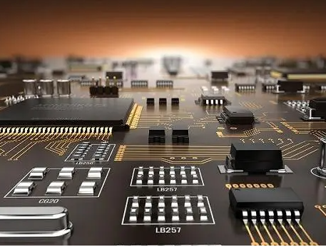
Professional PCB manufacturing and assembly
Building 6, Zone 3, Yuekang Road,Bao'an District, Shenzhen, China
+86-13410863085Mon.-Sat.08:00-20:00

The circuit and principle of the two parts on MTK6225 platform are introduced in detail. The first part is the RF part. The main chip selected is MT6139, and the RF structure used is a very low IF structure. From the signal direction, RF can be divided into two parts: reception and transmission. The basic modules include antenna, RF connector, acoustic surface filter, antenna matching circuit, transceiver MT6139, power amplifier, crystal oscillator, and RF power supply circuit. This paper draws the basic schematic diagram of each module and peripheral matching circuit through understanding the overall radio frequency. In terms of baseband, its basic modules include audio module, charging module, memory module, camera module, main screen LCD module, multimedia card interface module, SIM card module, USB module, keyboard and key light module, motor drive and Hall switch module, etc. This paper also draws the schematic diagram of each module of baseband in detail.
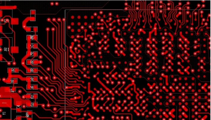
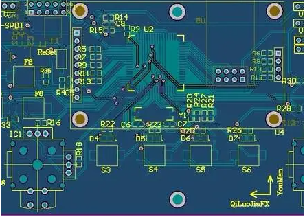
2. After realizing the schematic diagram, this paper also further completed the production of six layers of PCB. Through the skillful use of the EDA tool PADS, the RF and baseband parts of the PCB layout are rationalized to ensure that the important signal lines (RF lines, audio lines, etc.) do not interfere with each other. And on this basis, under the constraints of various detailed rules, optimize and reasonable wiring to ensure that all kinds of protection processing of some important signal lines, such as power supply, RF, audio, can be completed, so as to ensure the function and performance of PCB development board, and prepare for later testing.
3. Finally, a relatively complete RF test and baseband function test were carried out on the mobile phone development board, and the RF report of the mobile phone was given, including the receiving sensitivity test report, frequency error test report, phase error test report, output power test report, transmission carrier envelope test report, and modulation spectrum and switch spectrum test report, According to the test report, modify and debug the schematic diagram or PCB to improve some data in the report that does not conform to the GSM communication protocol. In the baseband, some hardware problems encountered in the test are given, and the work done to solve these problems is explained.
MTK design
GSM mobile phone is a typical complex embedded system. Its development includes microwave RF technology, digital signal processing and coding technology, smart card, real-time operating system, communication protocol and many other software and hardware technologies. At the same time, the development of GSM mobile phones can have different modes, including peripheral technology development, core technology development and basic technology development. The core technology of mobile phones is RF unit design, baseband unit design and protocol PCB software design. The peripheral design technology of mobile phones is modeling design and human-computer interface software design, The development of basic technology is mainly the development of baseband special chips and the design of physical layer software (including voice signal compression coding, decoding, channel coding, encryption, etc.). From the hardware point of view, the design of RF chip and baseband chip is one of the core technologies of mobile terminal system.
In recent years, most of the mobile phones we contact are GSM mobile phones. This paper introduces the hardware implementation principle and production process of GSM mobile phones. The mobile phone hardware module introduced in this paper is based on MTK GSM module, which includes baseband processing of GSM system and RF signal receiving and transmitting part. From the content, we will first introduce the GSM communication system, the basic principle of GSM mobile phone, and the schematic diagram of each module. At the same time, we will expand the functions and optimize the performance based on the existing platform according to the customer's requirements.
In addition, PCB wiring is an important part of the overall design of mobile phones. Mastering this PCB technology will enable us to master part of the sovereignty of mobile phone localization. In the process, electromagnetic compatibility is a very difficult problem. On dozens or dozens of square centimeters of circuit boards, the frequency changes greatly, and the level signals include small signals of microvolt magnitude and large signals of several watts of power, It is difficult and challenging to avoid their interference. In addition, it is also a difficult problem to eliminate the distortion in the signal transmission process, for high-frequency signals.


Just upload Gerber files, BOM files and design files, and the KINGFORD team will provide a complete quotation within 24h.