
Professional PCB manufacturing and assembly
Building 6, Zone 3, Yuekang Road,Bao'an District, Shenzhen, China
+86-13410863085Mon.-Sat.08:00-20:00

A PCB designmainly includes defining product requirements, PCB hardware system design, device selection, PCB drawing, PCB production proofing, welding debugging and other steps. What should be paid attention to in these steps? Xiao Bian will take you to fine articles, and must do so!
1、 Clarify requirements
At the beginning of a hardware PCB design, the first thing to do is to define the product requirements, which mainly includes defining the functional requirements and shape. The main functions need to be clarified. A few additional functions can be added later, but the main functions of the product cannot be affected. The determination of product shape is very important, which will affect the later PCB drawing and component selection.
2、 Hardware system design
The hardware system design shall determine the power supply mode, sensor type, communication mode, human-computer interaction mode, reserved interface, etc. of the product according to the functional requirements of the product. Generally, Visio can be used to draw the system block diagram. The system block diagram should be able to describe the relationship between each module circuit of the hardware system and the module components of the whole system.
3、 Device selection
At this stage, relevant devices need to be selected according to their own product functions, generally including the selection of power supply, master control, sensor, communication, storage and other chips. The selection needs to consider the function, price, supply and other factors of the chip to select a chip suitable for your product. The selection channels of chips can be compared through large chip electronic component stores such as Lichuang Mall, Yunhan Core Mall, and Dejie Electronics.
PCB design
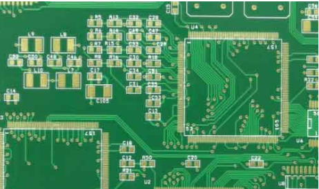
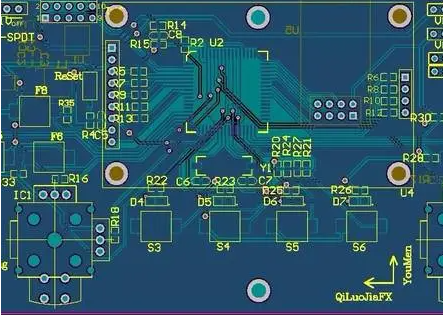
4、 PCB drawing
The EDA software involved in PCB drawing. At present, the mainstream PCB design tool software used by domestic engineers and technicians engaged in circuit design are Allegro, PADS and Altium Designer. Beginners recommend Altium Designer. There will be more online tutorials.
5、 PCB production proofing
After the PCB is designed, you can go to the PCB manufacturer for proofing. Before production, you need to provide the manufacturer with production documents. One way is to directly provide PCB documents. This method will have the risk of product leakage, so it is safer to provide gerber documents. The price of sample proofing is generally 50-100 yuan, and the delivery time is generally 24 hours. Of course, special PCB will be different. It is recommended to go to Huaqiang PCB, Jialichuang, Jiepei and other large manufacturers for proofing to avoid abnormal debugging due to PCB production problems. This situation will lead you to doubt life later.
6、 PCB welding test
After PCB and components are in place, they can be welded. Necessary tools for welding: soldering iron and air gun. Whether tweezers are needed or not depends on the technology. Welding is generally divided into direct manual welding and brushing steel mesh welding. Direct welding tests the technology, and the welding is not beautiful. If the steel mesh is brushed for welding, you can place an order for the steel mesh together during PCB production. Generally, a steel mesh is 50. After painting solder paste on the steel mesh, mount the patch on the machine if conditions permit, or put it manually if not. Arrange a furnace for reflow soldering, or blow it with an air gun.


Just upload Gerber files, BOM files and design files, and the KINGFORD team will provide a complete quotation within 24h.