
Professional PCB manufacturing and assembly
Building 6, Zone 3, Yuekang Road,Bao'an District, Shenzhen, China
+86-13410863085Mon.-Sat.08:00-20:00


First of all, a basic introduction is given. The number of layers of PCB can be divided into single layer, double layer and multi-layer. Single layer is basically eliminated now. Double layer boards are widely used in audio systems. They are generally used as coarse power amplifier boards. Multilayer boards refer to boards with four or more layers. Generally speaking, four layers are enough for components with low density requirements. From the perspective of via, it can be divided into through hole, blind hole and buried hole. A through-hole is a hole that passes directly from the top layer to the bottom layer; The blind hole is penetrated from the top or bottom hole to the middle layer, and then it is not penetrated any more. The advantage is that the location of this hole is not blocked from head to tail, and other layers can still route at the location of this hole; The buried hole means that the vias are buried from the middle layer to the middle layer, and the surface is completely invisible.
Before automatic wiring, wires with high requirements shall be wired interactively in advance. The side lines of input and output terminals shall not be adjacent and parallel to avoid reflection interference. If necessary, ground wires can be added for isolation, and the wiring of two adjacent layers should be perpendicular to each other, because parallel is easy to generate parasitic coupling. The routing rate of automatic routing depends on good layout, and the routing rules can be preset, such as the number of routing bends, the number of through holes, and the number of steps. Generally, exploratory routing is carried out first to quickly connect the short lines, and then through labyrinth routing to optimize the global routing path of the lines to be laid. It can disconnect the already laid lines as needed and try to re route them, so as to improve the overall routing effect.
For the layout, one principle is to separate the digital and analog as far as possible, so that the low speed should not be close to the high speed. The most basic principle is to separate digital grounding from analog grounding. Digital grounding is a switching device, and the current is large at the moment of switching, but small when it is not moving, so digital grounding cannot be mixed with analog grounding.
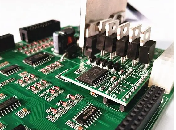
PCB design drawing
1. Precautions for wiring between power supply and ground wire
(1) Coupling capacitance shall be added between power supply and ground wire. Make sure that the power supply is connected to the pin of the chip after passing through the decoupling capacitor. The following figure lists several wrong connection methods and a correct connection method. Do you make such a mistake by reference? Decoupling capacitors generally have two functions: one is to provide instantaneous large current to the chip, and the other is to remove power supply noise. On the one hand, the power supply noise should not affect the chip as much as possible, and on the other hand, the noise generated by the chip should not affect the power supply.
(2) Widen the power supply and ground wire as much as possible. It is better to make the ground wire wider than the power line. The relationship is: ground wire>power line>signal line.
(3) You can use a large area of copper layer as the ground wire, and connect the unused places to the ground on the printed board for use as the ground wire, or make it into a multilayer board, with one layer for power supply and one layer for ground wire.
2. Processing when digital circuit and analog circuit are mixed
Now, many PCBs are no longer single function circuits, but are composed of digital circuits and analog circuits. Therefore, when wiring, it is necessary to consider the mutual interference between them, especially the noise interference on the ground wire.
Due to the high frequency of digital circuits and strong sensitivity of analog circuits, high frequency signal lines should be as far away from sensitive analog circuit devices as possible for signal lines, but for the entire PCB, the ground wire of the PCB can only have one node to the outside, so the problem of common ground between digital circuits and analog circuits must be handled inside the PCB, while inside the circuit board, the ground of digital circuits and the ground of analog circuits are actually separated, Only at the interface between PCB and the outside world (such as plug). There is a short circuit between the ground of the digital circuit and the ground of the analog circuit. Please note that there is only one connection point, and some are not grounded on the PCB, which is determined by the system design. 3. Treatment of line corners
Generally, the thickness of the line will change at the corner, but when the diameter of the line changes, some reflection will occur. For the change of line thickness, the right angle is the worst, the 45 degree angle is better, and the fillet is the best. However, rounded corners are troublesome for PCB design, so it is generally determined by the sensitivity of the signal. Generally, 45 degree angles can be used for signals. Only those very sensitive lines need rounded corners.
4. Check the design rules after wiring
No matter what we do, we should check it after we finish it. Just like when we have time left in the exam, we should check our answers. This is an important way for us to get high scores. Similarly, we draw PCB boards. In this way, we can be more sure that the circuit boards we draw are qualified products. We generally check the following aspects:
(1) Whether the distance between line and line, line and component pad, line and through-hole, PCB component pad and through-hole, through-hole and through-hole is reasonable and meets production requirements.
(2) Whether the width of the power line and ground wire is appropriate, whether the power line and ground wire are tightly coupled (low wave impedance), and whether there is a place in the PCB where the ground wire can be widened.
(3) Whether the best measures have been taken for the key signal lines, such as the shortest length, adding protective lines, and the input lines and output lines are obviously separated.
(4) Whether the analog circuit and digital circuit have their own independent ground wires.
(5) Whether the graphics (as shown in the figure and marked) added in the PCB will cause signal short circuit.
(6) Modify some undesirable alignments.
(7) Whether there is process line added on PCB, whether the solder mask meets the requirements of PCB production process, whether the solder mask size is appropriate, and whether the character mark is pressed on the PCB device pad to avoid affecting the electrical assembly quality.
(8) Whether the outer frame edge of the power supply layer in the multilayer PCB is shrunk, for example, if the copper foil of the power supply layer is exposed outside the board, it is easy to cause a short circuit.
In a word, the above skills and methods are based on experience, which is worth learning when drawing PCB boards. In addition to skillfully using drawing tools and software, you should also have solid theoretical knowledge and rich practical experience, which can help you complete your PCB drawings quickly and effectively. But it is also very important to be careful. Every step of wiring and overall layout should be taken seriously, because a small error may lead to your final product becoming a waste product, and then we can't find any errors. So we would rather spend more time checking the details carefully than return to check when problems occur, That may take more time. In short, pay attention to the details in the process of drawing PCB.


Just upload Gerber files, BOM files and design files, and the KINGFORD team will provide a complete quotation within 24h.