
Professional PCB manufacturing and assembly
Building 6, Zone 3, Yuekang Road,Bao'an District, Shenzhen, China
+86-13410863085Mon.-Sat.08:00-20:00

One of the main purposes of circuit schematic design is to provide a network table for the design of PCB, and to prepare for the design of PCB.
The design process of multi-layer PCB is basically the same as that of ordinary PCB boards. The difference is that the wiring of the intermediate signal layer and the division of the internal electrical layer are required. In general, the design of multilayer pcb boards is basically divided into the following steps. This article first introduces these steps briefly.
The planning of circuit board is mainly to plan the physical size of pcb board, the packaging form of components, the installation mode of components, and the board structure, that is, single layer board, double layer board, and multilayer board.
Working parameter settings mainly refer to working environment parameter settings and working layer parameter settings. The correct and reasonable setting of pcb environment parameters can bring great convenience to the design of circuit boards and improve work efficiency.
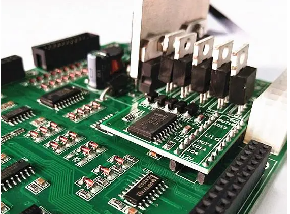
After the component layout and adjustment are completed in the current period, you can import the network table into the pcb, or you can directly import the network table by updating the pcb in the schematic diagram. Readers who have used protel dxp know that the system has its own automatic layout function, but the effect of the automatic layout function is often not ideal. Generally, manual layout should be used, especially for complex circuits and components with special requirements. The layout and adjustment of PCB components is an important work in the design of pcb, which directly affects the following operations such as wiring and internal electrical layer segmentation.
Pcb design
Definition and setting of the intermediate layer of PCB. This operation focuses on setting the specific layer structure in the layer stack manager of the software, mainly setting the number of intermediate signal layers and internal electrical layers, upper and lower structures, etc.
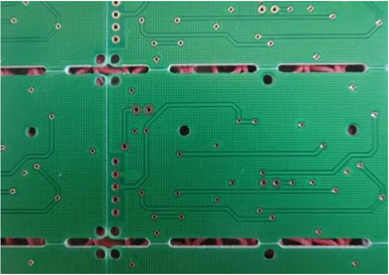
The internal power layer is divided. Generally, there is more than one power network in the internal power layer. It is often necessary to divide the internal power layer into several mutually isolated areas and connect each area to a specific power network. This is the biggest difference between multilayer boards and ordinary boards, and it is also an important link in the design of multilayer circuit boards. The structure of internal electric layer division often directly affects the routing of power and ground grids, and is also affected by component layout and routing.
The setting of wiring rules mainly refers to the setting of various specifications for circuit wiring, wire line width, parallel line spacing, safe spacing between wire and bonding pad, and via size. No matter what wiring method is adopted, wiring rules are an essential step. Good wiring rules can ensure the safety of circuit board wiring, meet the requirements of PCB manufacturing process, and save costs.
For wiring and adjustment, the system provides automatic wiring, but it often fails to meet the requirements of designers. In practical applications, designers often rely on manual wiring, or partial automatic wiring combined with manual interactive wiring to complete wiring. In particular, it should be noted that the layout and wiring as well as the PCB circuit board have the characteristics of the internal electrical layer. Although the layout and wiring have their own sequence, in PCB design projects, the layout of the circuit board is often adjusted according to the needs of the separation of the wiring and the internal electrical layer, or the wiring is adjusted according to the layout. Between them, it is a process of mutual consideration and mutual adjustment.
Other auxiliary operations, such as copper coating and teardrop filling, as well as document processing such as report output and saving and printing, can be used to check and modify PCB circuit boards, and can also be used as a list of purchased components.
Understand PCB design, drawing and wiring skills
Nov 04,2022


Just upload Gerber files, BOM files and design files, and the KINGFORD team will provide a complete quotation within 24h.