
Professional PCB manufacturing and assembly
Building 6, Zone 3, Yuekang Road,Bao'an District, Shenzhen, China
+86-13410863085Mon.-Sat.08:00-20:00

Basic Requirements for Wiring in High Speed PCB Design
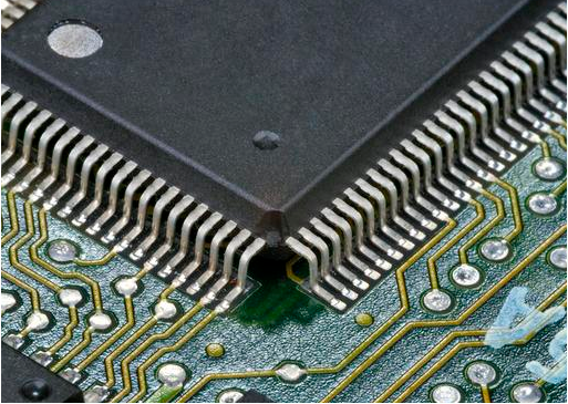
(1) The outgoing line of rectangular pad encapsulated by QFP, SOP, etc. shall be led out from the PIN center (generally using shape)
(2) The distance from the wiring to the board edge shall not be less than 20 MIL.)
(3) No other network via or surface wiring is allowed under the metal shell device (common metal shells include crystal oscillator, battery, etc.)
(4) Except for DRC errors caused by encapsulation itself, there shall be no DRC errors in wiring, including DRC errors in networks with the same name, except for compatible designs.
(5) After PCB design, there is no unconnected network, which is consistent with PCB network and circuit diagram network list.
(6) Dangline Line is not allowed.
(7) If it is clear that non functional pads do not need to be retained, they must be removed from the photo file.
(8) For high-speed pcb design, it is recommended that the distance from the wiring to the board edge should be greater than 2MM
(9) The design of high-speed pcb suggests that the inner layer wiring should be preferred for signal lines
(10) It is recommended that the corresponding power plane or ground plane in the high-speed signal area be kept as complete as possible
(11) It is recommended that PCB wiring is evenly distributed, and auxiliary copper is required for large areas without wiring, but it is required that impedance control is not affected
(12) It is recommended that all wiring be chamfered, and the recommended chamfering angle is 45 degrees
(13) It is recommended to prevent PCB signal lines from forming a self loop with a side length of more than 200MIL on adjacent layers
(14) It is recommended that the wiring direction of adjacent layers be orthogonal
Note: The wiring of adjacent layers of high-speed pcb is designed to avoid going in the same direction to reduce the cross talk between layers. If it is unavoidable, especially when the signal rate is high, the ground plane should be considered to isolate each wiring layer, and the ground signal should be used to isolate each signal line.
Through Hole Technology of PCB Proofing
Through hole is an important part of multilayer printed circuit board. Drilling cost usually accounts for only 30% to 40% of the PCB proofing cost. From this point of view, it is divided into two parts: a small part serves as the electrical connection between layers; The other part is used as a fixing device. From the perspective of PCB proofing process, through-hole can be divided into three types: blind hole, buried hole and through-hole.
Through hole refers to the hole through the whole circuit board, which can be used for internal interconnection, or as the installation and positioning hole of components. Because vias are easy to implement and cost less, most printed circuit boards use vias instead of the other two.
The blind hole is on the upper and lower surface layers of the pcb circuit board and has a corresponding depth. Used to connect surface circuit and inner circuit. The depth of the hole usually does not exceed a certain ratio (aperture).
Buried hole refers to the connecting hole in the inner layer of the pcb circuit board, which does not extend to the surface of the pcb circuit board. The above two types of holes are located inside the PCB. The through hole forming method is adopted before pressing, and there may be multiple inner layers overlapping during the through hole forming process.

Let's take a look at EMC's PCB design technology
Nov 04,2022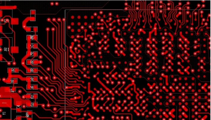


Just upload Gerber files, BOM files and design files, and the KINGFORD team will provide a complete quotation within 24h.