
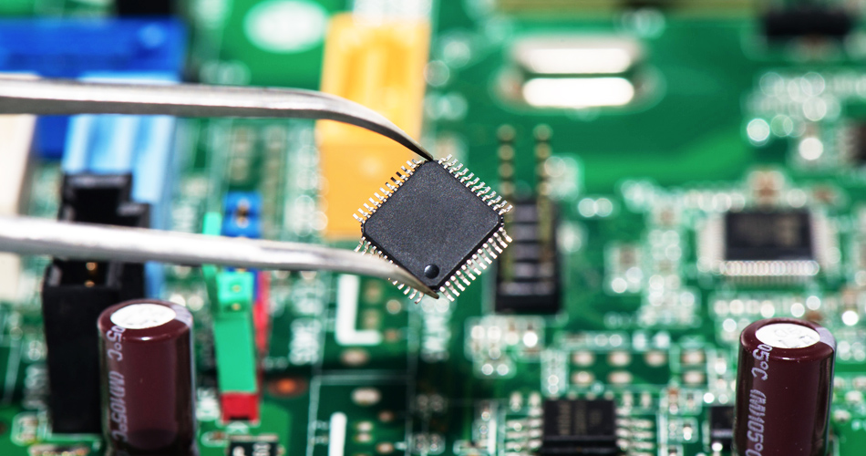
Professional PCB manufacturing and assembly
Building 6, Zone 3, Yuekang Road,Bao'an District, Shenzhen, China
+86-13410863085Mon.-Sat.08:00-20:00


PCBA engineers must see! 13 Key Points of Power Supply Design for RF Circuits
01
Power cord is an important way for EMI access circuit. Through the power line, external interference can be transmitted to the internal circuit, affecting RF circuit indicators. In order to reduce electromagnetic radiation and coupling, the loop area of primary side, secondary side and load side of DC-DC module shall be minimum. No matter how complex the power circuit is, its large current loop should be as small as possible. The power cord and ground wire should always be placed close together.
02
If switching power supply is used in the circuit, the layout of peripheral devices of switching power supply shall conform to the principle of shortest power return path. Filter capacitor shall be close to relevant pins of switching power supply. Use a common mode inductor near the switching power module.
03
Long distance power lines on a single board cannot be close to or pass near the output and input terminals of a cascade amplifier (with a gain greater than 45dB) at the same time. Avoid power lines becoming RF signal transmission channels, which may cause self excitation or reduce sector isolation. High frequency filter capacitors are required at both ends of long-distance power lines, and even in the middle.
04
Three filter capacitors are combined in parallel at the power supply inlet of the RF PCB to filter low, medium and high frequencies on the power line by taking advantage of their respective advantages. For example: 10uf, 0.1uf, 100pf. And close to the input pins of the power supply in order from large to small.
05
When feeding small signal cascade amplifiers with the same group of power supplies, power should be supplied from the last stage to the front stage in turn, so that the EMI generated by the last stage circuit has less impact on the previous stage. And each level of power filter has at least two capacitors: 0.1uf, 100pf. When the signal frequency is higher than 1GHz, add 10pf filter capacitor.
06
Commonly used for low-power electronic filters, the filter capacitor should be close to the triode pin, and the high-frequency filter capacitor should be closer to the pin. The triode with lower cut-off frequency shall be selected. If the triode in the electronic filter is a high-frequency tube, which works in the amplification area, and the layout of peripheral devices is unreasonable, it is easy to generate high-frequency oscillation at the power output.
The same problem may exist in the linear regulator module, because there is a feedback loop in the chip and the internal triode works in the amplification area. In the layout, the high-frequency filter capacitor shall be close to the pin to reduce the distributed inductance and destroy the oscillation condition.
07
The copper foil size of the POWER part of the PCB shall conform to the maximum current flowing through it, and allowance shall be taken into account (generally referred to as 1A/mm line width).
08
The input and output of the power cord cannot be crossed.
09
Pay attention to power decoupling and filtering to prevent interference from different units through power lines. During power wiring, power lines shall be isolated from each other. The power line shall be isolated from other strong interference lines (such as CLK) with ground wire.
ten
The power wiring of small signal amplifier needs to be isolated by grounding copper sheet and grounding via to prevent other EMI interference from entering, thus deteriorating the signal quality of this level.
eleven
Different power supply layers should avoid overlapping in space. It is mainly to reduce the interference between different power sources, especially between some power sources with large voltage difference. The overlapping problem of power plane must be avoided. If it is difficult to avoid, the interlayer can be considered.
twelve
The PCB layer allocation is convenient for simplifying the subsequent wiring processing. For a four layer PCB (a circuit board commonly used in WLAN), in most applications, the top layer of the circuit board is used to place components and RF leads. The second layer is used as a system, the power supply is placed in the third layer, and any signal line can be distributed in the fourth layer.
The second layer adopts a continuous ground plane layout, which is very necessary for establishing an impedance controlled RF signal path. It is also convenient to obtain the shortest ground loop as possible, providing a high degree of electrical isolation for the first and third layers, so as to minimize the coupling between the two layers. Of course, other board layer definitions can also be used (especially when the circuit board has different layers), but the above structure is a proven success example.
thirteen
Large area power supply layer can make Vcc wiring easier. However, this structure is often the fuse that causes system performance degradation. Connecting all power leads together on a large plane will not avoid noise transmission between pins. On the contrary, if star topology is used, the coupling between different power supply pins will be reduced. Good power decoupling technology combined with strict PCB layout and Vcc lead (star topology) can lay a solid foundation for any RF system design. Although there are other factors that can reduce the system performance in actual design, having a "noise free" power supply is the basic element to optimize the system performance.


Just upload Gerber files, BOM files and design files, and the KINGFORD team will provide a complete quotation within 24h.