
Professional PCB manufacturing and assembly
Building 6, Zone 3, Yuekang Road,Bao'an District, Shenzhen, China
+86-13410863085Mon.-Sat.08:00-20:00

The circuit board manufacturer will explain the cause and hazard analysis of faulty soldering in PCBA processing
According to statistics, nearly half of the failures of electronic products are caused by poor welding, which almost exceeds the probability of failure of electronic components. It reduces the reliability of electronic products, increases the noise, degrades technical indicators, and even makes the circuit board unable to complete the design function. More seriously, it leads to the sudden collapse of the entire system without any warning, causing significant economic losses and reputation losses.
In the testing link of electronic product production and after-sales maintenance link, the failure caused by faulty soldering causes a great waste of time and energy for technicians. Sometimes it is not uncommon to spend a whole day to find a faulty soldering point.
In the production process and maintenance process of electronic products, even if efforts are made in all aspects, the phenomenon of faulty soldering cannot be eradicated. Therefore, faulty soldering has always been the focus of the electronic industry.
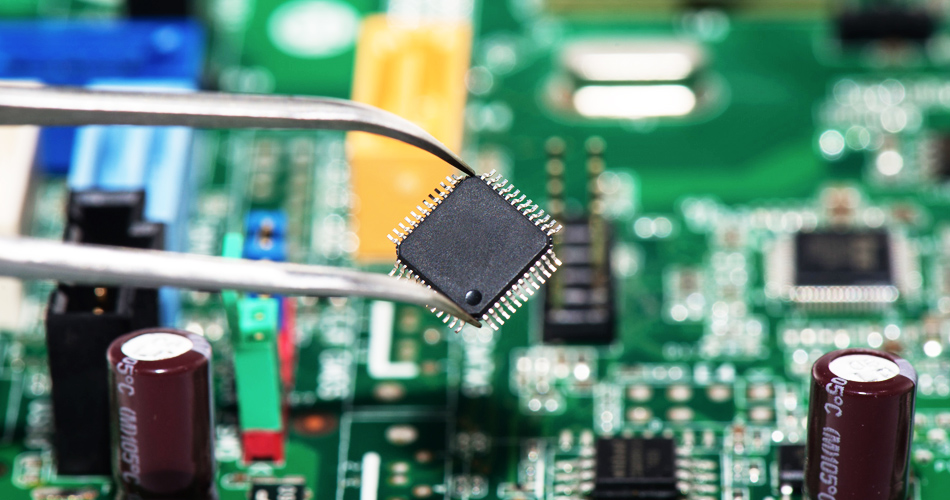
False soldering: one of the bad solder joints produced during the assembly process of electronic products. The welding interface of the solder joint does not form a good intermetallic compound (IMC), which makes an unreliable connection between the components and the substrate. (The false soldering defined here refers to the false soldering of solder joints on PCBA.)
Cause: the solderable surface of the substrate and the solderable surface of the electronic components are oxidized or polluted; Poor solder performance, poor flux performance, and poor substrate pad metal coating; Improper setting of welding parameters (temperature and time).
Impact: The faulty soldering makes the solder joint become a connection state with contact resistance, resulting in abnormal circuit operation, or the unstable phenomenon that the power is not connected when the electrical connection occurs, and the noise in the circuit (especially in the communication circuit) increases without regularity, which brings major hidden dangers to the debugging, use and maintenance of the circuit. In addition, some of the solder joints are not easy to find because they keep good electrical contact for a long time after the circuit starts to work. However, under the action of environmental conditions such as temperature change, humidity change and vibration, the contact surface is gradually oxidized, and the contact slowly becomes incomplete, thus making the circuit "strike". In addition, the contact resistance of the faulty solder joint will cause local heating, and the local temperature rise will further worsen the situation of the incomplete solder joint, eventually even make the solder joint fall off, and the circuit can not work normally. This process can sometimes take one or two years.
In the production and maintenance service of electronic products, it is not easy to find the faulty solder joints from an electronic device with thousands of solder joints. Therefore, faulty soldering is a hidden danger of circuit reliability, which must be paid attention to, and its laws must be studied to take measures to reduce its harm.
Features of faulty soldering: From the perspective of electronic product testing, some of the faulty solder joints in the production testing link show the characteristics of "time to time". Although it is difficult to find the fault, the faulty solder joints can be solved before leaving the factory; On the other hand, the open circuit phenomenon of faulty solder joints often occurs in a year or even longer, which makes the product stop working and cause losses.
Due to its concealment, accident occurrence and the significance of system collapse loss, faulty soldering cannot be ignored.
To study the causes of faulty soldering and reduce its harm is an important subject that must be paid attention to in the development of China from a large electronics manufacturing country to a powerful electronics manufacturing country.
Causes and prevention of false welding:
1. False soldering caused by component factors and its prevention:
Inadequate thickness, oxidation, pollution and deformation of the metal coating on the weldable parts of the components can cause the result of faulty soldering.
1.1. The thickness of the metal coating of the weldable part is not enough
Generally, the solderable surface of components is coated with a silver white, uniform and easily solderable tin layer of a certain thickness. If the coating is too thin or uneven, and copper based tin plating or steel based copper plating and then tin plating, the copper tin interface formed by the mutual contact between copper and tin will infiltrate each other for a long time to form an alloy layer diffusion, which will make the tin layer thinner, leading to a decrease in the solderability of the soldered surface. (Solderability refers to the ability of metal surface to be wetted by molten solder.) Buying components from large companies with long-term good cooperation can reduce the risk of faulty soldering caused by this reason.
1.2. Oxidation of solderable surfaces of components
Long storage time or improper storage conditions of electronic components can cause oxidation on the surface of electronic components' pins or welding ends, resulting in faulty soldering. The oxidized welding surface is gray and black, and serious oxidation can be detected by visual inspection. The oxidized electronic components can be discarded or reused after the oxidation treatment is qualified. Generally, the oxide layer shall be wiped and scraped by external force; Slightly acid cleaning; Apply flux, and then use tin coating. (Surface mounted components are generally difficult to handle due to their small package size and oxidation, so they are usually returned to the manufacturer for replacement or scrapping)
In addition to visual inspection, there are more complex and detailed solderability test and detection standards for whether components are oxidized. If conditions are not met, components can be sampled and welded in batches by manual, wave soldering or reflow soldering methods.
1.3. Contamination of solderable surfaces of components
In the production of electronic products, components must go through such processes or operations as incoming material receiving and counting, storage, issuing, forming and plug-in (THT process), SMC and SMD loading and unloading, mounting and manual repair welding, which will inevitably produce dust, oil and sweat contamination, resulting in a decline in the solderability of electronic component welding surface.
In the electronic assembly and assembly production site, keeping a clean production environment, wearing protective equipment and operating in strict accordance with the operating procedures are effective measures to prevent component pollution.
1.4. Component pin deformation
SMD devices, especially QFP and SOP packaging devices with thin pin spacing, are easy to damage and deform the pins, and the coplanarity of the pins becomes poor. After mounting, some pins do not cling to the bonding pad, causing false soldering.
Prevention: For the fine pitch IC mounting, use special tools to take and place the IC. Remember not to touch the pin directly with your hand. During the operation, prevent the IC from falling. QFP is commonly used for disk mounting. SOP is generally rod packaging (do not bend during production). After the IC pin is deformed, it should be reshaped and checked before mounting. (For example, QFP can be corrected and checked on flat steel plate or glass)
2. False soldering caused by substrate (usually PCB) factors and its prevention:
In the process of electronic assembly, the oxidation, pollution and deformation of PCB can cause false soldering. (The unreasonable design of PCB insertion holes and pads is also one of the causes of false soldering, which will not be discussed here.).
2.1. False soldering caused by PCB oxidation and prevention
The PCB may be oxidized on the wall of the pad and the insertion hole due to long storage time or improper storage conditions, resulting in false soldering.
The oxidized bonding pad loses its metallic luster, turns gray and black, and there is no abnormal condition through visual inspection. For PCB suspected to be oxidized, the solderability test shall be carried out according to the standard, and the PCB can be used only when the result is good. The following are PCB storage conditions, storage life and baking conditions for various surface treatments:
Silver plate: storage conditions before and after vacuum packaging: temperature<30 ℃, relative humidity<60%. Effective storage time after vacuum packaging is half a year to one year When the storage time is more than six months, in order to avoid bursting caused by the moisture stored in the plate, the moisture inside the plate is usually removed by baking after unpacking, and the baking condition is 120 ℃ for one hour (The maximum time shall not exceed 2 hours), use a clean special oven, and cover the top and bottom sides of the silver plate with aluminum foil paper to avoid oxidation of the silver surface or dielectric absorption pollution
OSP board: storage conditions before and after vacuum packaging: temperature 20~30 ℃, relative humidity<50% The effective storage time after vacuum packaging is 3 months to 1 year When the storage time is more than six months, in order to avoid bursting caused by moisture stored in the plate, the moisture inside the plate is usually removed by baking after unpacking, and the baking condition is 110~120 ℃, 1 hour (the longest time shall not exceed 1.5 hours)
Metallizing plate: storage conditions before and after vacuum packaging: temperature<30 ℃, relative humidity<60%. The effective storage time after vacuum packaging is half a year When the storage time is more than six months, in order to avoid bursting caused by the moisture stored in the plate, the moisture inside the plate is usually removed by baking after unpacking, and the baking condition is 120 ℃ for one hour (The maximum time shall not exceed 2 hours) Storage conditions before and after vacuum packaging: temperature<25 ℃, relative humidity<60%. The effective storage time after vacuum packaging is one year When the storage time is more than six months, in order to avoid bursting caused by the moisture stored in the plate, the moisture inside the plate is usually removed by baking after unpacking, and the baking condition is 120 ℃, 1 hour (the longest time shall not exceed 1.5 hours)
2.2. False soldering caused by PCB pollution and prevention:
In the production process of PCB boards, operators must contact with PCB in PCB receiving, storage, SMT printing, SMT mounting, THT plug-in, wave soldering and other processes. Dust, oil and sweat will pollute the pad, thus reducing the solderability of PCB and causing false soldering.
It is a good habit to avoid PCB pollution to maintain a clean production environment and operate according to the production process operating procedures.
PCB found to be contaminated shall be cleaned, decontaminated and dried before use.
2.3. False soldering caused by PCB deformation and prevention:
After PCB deformation, the coplanarity of component mounting becomes worse, and some component pins and pads are suspended in the air (the distance is small, otherwise empty soldering may occur), causing false soldering. In particular, BGA and QFP packaging components in SMT process are more likely to form faulty soldering.
There are generally two cases of PCB deformation: first, incoming materials are deformed, and the incoming materials are checked and accepted according to the standard.
For PCB warpage standard, please refer to Article 2.11 Flatness Standard of IPC-A-600G: for printed boards with surface mounted components (such as SMT mounting), the twist and bow standard shall not be greater than 0.75%, and for other types of boards, it shall not be greater than 1.5% Refer to IPC-TM-650 2.4.22 for test method
2.4 The solderable layer on the PCB surface has different process treatment methods and different metal materials, and its solderability indicators are also different. If the solderability indicators are not qualified, it is also a major reason for faulty soldering.
2.5. Some PCBs were warped and deformed during the high temperature period of reflow soldering, and returned flat after cooling, resulting in faulty soldering and high stress. The possibility of solder joint failure in the later period was very high.
3. False Soldering Caused by Flux and Solder and Its Prevention
3.1. False soldering caused by flux and prevention
In the THT or SMT and THT mixed packaging process, the soldering flux shall be coated before wave soldering. If the performance of the soldering flux is poor, the oxide on the component welding surface and PCB insertion holes and pads cannot be effectively removed, resulting in faulty solder joints. Special attention shall be paid when changing the manufacturer or model of flux. Especially when new type flux is used, welding test shall be conducted.
The concentration of flux shall be checked frequently and updated according to the process specification.
3.2. False soldering caused by solder factor and its prevention
In the wave soldering sequence, the tin lead solder is continuously oxidized at a high temperature of 250 ℃, which makes the tin content of the solder continuously decrease and deviate from the eutectic point, resulting in poor liquidity of the solder, faulty soldering and insufficient solder joint strength. The following methods can be used to solve the problem.
Adding oxidation-reduction agent can reduce oxidized SnO to Sn and reduce the production of tin slag; Continuously remove solder dross; Add a certain amount of tin before each welding; Solder containing oxidation resistant phosphorus is used; Nitrogen protection welding is adopted to isolate the solder from the air, so as to greatly reduce the generation of scum.
At present, the better method is to use phosphorus containing solder under nitrogen protection, which can control the scum rate to the lowest degree and minimize welding defects.
In the SMT process, the reflow welding sequence, the solder paste will also be continuously oxidized in use, and the metal content in it will become lower and lower, or the flux in it will become less, which will also cause faulty welding. Reasonable selection of reflow temperature curve can reduce the occurrence of faulty soldering.
Improper matching between solder and PCB metal layer, solder and component leg metal layer will also cause faulty soldering.
When the lead solder is mixed with the lead-free solder end, if the temperature curve of the lead solder is used, the lead solder is melted first, but the lead-free solder end cannot be completely melted, so that the interface at one side of the component cannot generate a good intermetallic alloy layer, so the welding quality is the worst when the lead solder is mixed with the lead-free solder end. In this case, the welding temperature can be increased to 230~235 ℃.
4. False welding caused by other factors and its prevention:
4.1. In the process of wave soldering and reflow soldering solder cooling and solidification, PCBA jitter produces disturbed solder joints with low strength. Solder joints are prone to open circuit and failure during customer use. In electronic assembly, this situation is also often classified as faulty soldering.
4.2. When the PCBA has large bending, it is fixed on the chassis base during product assembly, and the PCBA is forced to be flat, causing stress, and the solder joint will crack over time, leading to open circuit. (Strictly speaking, this should be the late failure of the solder joint, which belongs to the generalized faulty soldering.). The preventive method is to use PCB with qualified flatness. If the hot plate is bent because it is not laid flat when wave soldering and reflow soldering are out of the furnace, it can be restored to flatness by another wave soldering or reflow soldering. Remember to correct the bending manually.
4.3. Another case is that the PCBA is flat, but its fixed base is uneven (theoretically, there are N fixed bases, and generally only three are on the same plane). The installation effect is the same as that in 2).
The installation base should be flat, and the number of fixed seats of PCBA should not be as large as possible, which can meet the requirements of fixed strength. The more fixed seats, the more severe the slight unevenness after PCBA installation.
4.4. In the parts of the circuit board that are often subjected to external forces in use, such as the solder joints near the key switch on the PCBA, it is very easy to cause metal fatigue due to slight bending during use, leading to solder joint failure (the result is the same as solder joint failure).
4.5. The solder joints near the heating elements on the PCBA are relatively easy to fail and open, and the effect is the same as that of faulty soldering.
4.6. In the production process of PCB, remember to prevent bending, otherwise cracks will appear on the through hole metallized wall, which will lead to the phenomenon of time connection and time gap, and it is very easy to misjudge with false soldering.
Power supply design of rf circuit
Oct 27,2022


Just upload Gerber files, BOM files and design files, and the KINGFORD team will provide a complete quotation within 24h.