
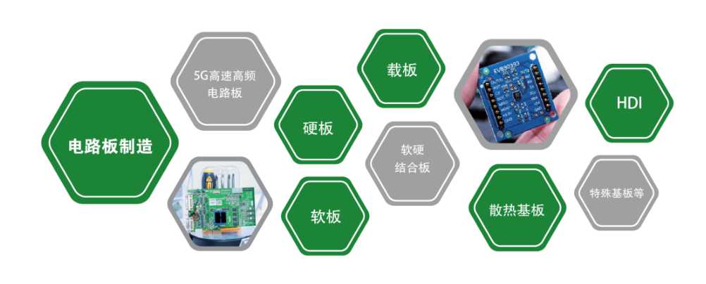
Professional PCB manufacturing and assembly
Building 6, Zone 3, Yuekang Road,Bao'an District, Shenzhen, China
+86-13410863085Mon.-Sat.08:00-20:00


From the above two formulas, we can see that the total noise of the far end crosstalk subsides each other due to the polarity relationship of capacitive and inductive coupling, that is, the far end crosstalk can be eliminated. In PCB wiring, Stripline circuits can show a good balance between inductive and capacitive coupling, and the forward coupling energy is very small. As for microstrip wire, most of the electric field associated with crosstalk passes through air rather than other insulating materials, so capacitive crosstalk is smaller than inductive crosstalk, resulting in a small negative forward coupling. This is the reason why the interference of the far end crosstalk is often ignored in the general design, and the improvement of the near end crosstalk is emphasized.
In the actual design, the relevant parameters of PCB (such as thickness, dielectric constant, etc.), line length, line width, line distance, transmission line and ground plane position and current flow direction will affect the size of c, l, Cm, Lm, L, and the signal frequency and device rise/fall time.
Here we do not do the quantitative analysis of the influence of these parameters on the crosstalk, the relationship between these parameters and the degree of their influence on the crosstalk.

2.4 Changing trend of crosstalk
The magnitude of mutual inductance and mutual capacity affects the magnitude of crosstalk and thus changes the characteristic impedance and propagation velocity of transmission line equivalently. Similarly, the geometry of the transmission line greatly affects the variation of mutual inductance and mutual capacitance, so the characteristic impedance of the transmission line itself also has an effect on these parameters. In the same medium, relatively low-impedance transmission lines are more strongly coupled to the reference plane (ground plane) and less coupled to neighboring transmission lines, so that low-impedance transmission lines have less impedance change due to crosstalk.
3. Several effects caused by crosstalk
In high speed, high density PCB design, a complete ground plane is generally provided, so that each signal line basically only interacts with its nearest signal line, and the cross coupling from other distant signal lines can be ignored. Nonetheless, in analog systems, very high crosstalk resistance is required when a high-power signal passes through a low-level input signal or when a component with a higher signal voltage (such as TTL) is in close proximity to a component with a lower signal voltage (such as ECL). In PCB design, crosstalk has two typical effects on the signal integrity of high-speed PCBS if not handled correctly.
3.1 False trigger caused by crosstalk
Signal crosstalk is an important part of signal integrity problem in high-speed design. The function error caused by crosstalk is the most common one.
A typical transmission of adjacent network error logic caused by crosstalk pulses. The signal transmitted on the source network is transmitted through the coupling capacitor, causing a noise pulse in the interfered network and at the receiving end. As a result, an unwanted pulse is sent to the receiving end. If the pulse intensity exceeds the trigger value of the receiving end, uncontrollable trigger pulses will be generated, causing the logical function of the next level of network chaos.
3.2 Timing delay caused by crosstalk
Timing is an important consideration in digital design. Figure 5 shows timing problems caused by crosstalk noise. The lower part of the figure is helpful for the two noise pulses (delay glitch and Unhelpful glitch caused by crosstalk noise) generated by the interference source network. When the noise pulses are superimposed on the interfered network, the signal transmission delay of the interfered network is reduced. Similarly, when noise pulses (Unhelpful glitch) are superimposed on the disturbed network, it increases the delay in the normal transmission of signals by the disturbed network. Although such crosstalk noise reducing network transmission delay is helpful to improve PCB timing, in actual PCB design, due to the uncertainty of interference source network, such delay cannot be controlled, so the delay caused by such crosstalk must be suppressed.
4. Minimize crosstalk
Crosstalk is common in high speed and high density PCB design, and the effect of crosstalk on the system is generally negative. To reduce crosstalk, it is essential to minimize the coupling between the source network and the interfered network. It is impossible to avoid crosstalk completely in high density complex PCB design, but in system design, designers should choose appropriate methods to minimize crosstalk without affecting other system performance. Based on the above analysis, crosstalk problem is mainly solved from the following aspects:
As far as possible, the distance between transmission lines should be extended if the wiring conditions permit. Or minimize the parallel lengths between adjacent transmission lines (cumulative parallel lengths), preferably between different layers.
The direction of the two adjacent signal layers (without isolation of the plane layer) should be vertical. Parallel routing should be avoided to reduce cross-talk between layers.
Under the condition of ensuring signal timing, devices with low conversion speed should be selected as far as possible to slow down the changing rate of electric and magnetic fields, thus reducing crosstalk.
In the design of the cascade, the dielectric layer between the wiring layer and the reference plane (power or ground plane) should be as thin as possible under the condition of satisfying the characteristic impedance, so as to increase the coupling degree between the transmission line and the reference plane, and reduce the coupling of adjacent transmission lines.
Because the surface layer has only one reference plane, the electric field coupling of the surface layer wiring is stronger than that of the middle layer, so the signal lines that are more sensitive to crosstalk should be distributed in the inner layer as far as possible.
The amplitude of crosstalk can be greatly reduced by terminating the impedance of the far end and the near end of the transmission line to match the transmission line.
Digital system design has entered a new stage. Many high-speed design issues that used to be secondary now have a critical impact on system performance. The problems of signal integrity, including crosstalk, bring about changes in design concepts, design processes and design methods. In the face of new challenges, for the crosstalk noise, the most critical is to find those networks that have a real impact on the normal operation of the system, rather than blind suppression of all networks crosstalk noise, which is also contradictory with limited wiring resources. The crosstalk problem discussed in this paper is very important to solve the crosstalk problem in high speed and high density circuit design.
PCB production process
Jun 02,2023


Just upload Gerber files, BOM files and design files, and the KINGFORD team will provide a complete quotation within 24h.