
Professional PCB manufacturing and assembly
Building 6, Zone 3, Yuekang Road,Bao'an District, Shenzhen, China
+86-13410863085Mon.-Sat.08:00-20:00


PCB production process
The minimization of all solder joint defects should be the goal of any SMT manufacturer. By understanding defects, their root causes and how to prevent SMT placement defects, you can greatly improve the quality of all the components you manufacture. According to industry statistics, the top three PCBA assembly defects account for 74% of all manufacturing defects, including short circuits, virtual soldering and component displacement.
Weld 44%
A solder joint occurs when there is no connection between the lead and the pad or other connection points on the PCB result in an open connection. It can also happen when the solder is only present on the PCB pads and there is no solder on the component leads.
Bridge welding bridge (short circuit) 15%
A short circuit, sometimes called solder bridging, occurs when solder incorrectly crosses over and connects one lead to the other. This short dimension can be microscopic and very difficult to detect. If a short is not detected, serious damage to circuit components can occur, such as burnt or blown components and/or burned PCB traces. Components offset by 15%
Component drift can be described as a misalignment of an item with its target. Component displacement can occur during reflow due to the ability of components to float on molten solder. Components with many pads (such as BGA components) may rearrange due to the surface tension of the molten solder, but many times the components will remain where they were placed, which is a good reason to ensure components are placed exactly where they assume In the middle of the pad or land area.
First, let's understand a few concepts:
(1) UNIT: UNIT refers to the unit graphics designed by PCB design engineers.
(2) SET: SET refers to an overall graphic that engineers put together multiple UNITs in order to improve production efficiency and facilitate production. That is what we often call jigsaw, which includes unit graphics, process edges and so on.
(3) PANEL: PANEL refers to a board composed of multiple SETs combined with tool board edges for reasons such as improving efficiency and facilitating production when PCB manufacturers produce.
(4) Dry film: Dry film is the process of transferring the circuit pattern to the PCB board.
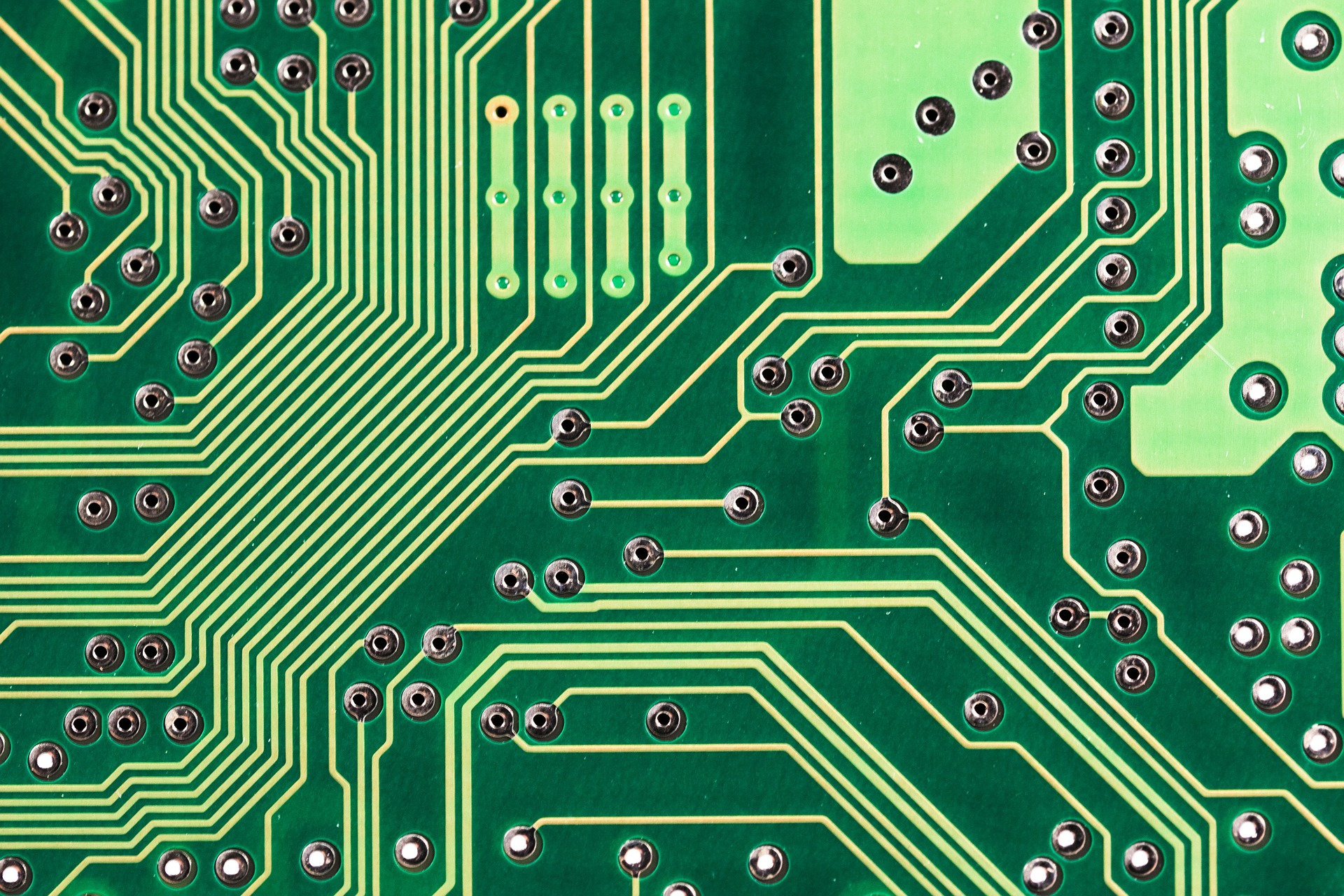
The concept of graphics transfer will be mentioned in PCB production, because the production of conductive graphics is the foundation of PCB production. Therefore, the graphics transfer process is of great significance to PCB production.
The wet film process and manual line in the PCB industry still occupy a very high market due to their cost factors. However, as many customers pay more attention to quality, wet film process and manual line will be gradually eliminated. Jiali Chuang has already fully entered the era of automatic line dry film. It is the first manufacturer in Shenzhen and even the whole country to focus on small batches and prototypes; it is the first manufacturer to adopt fully automatic line dry film technology!
The entire process flow of PCB is shown in the figure below.
1. Cutting, filleting, chamfering
Cutting is the process of cutting the original copper clad laminate into boards that can be made on the production line, generally cutting into work boards of about 40*50cm.
2. Drilling
The effect of drilling the hole is shown in the figure, because it is difficult to use a camera to take pictures of the situation inside the hole, and there is no copper in the hole at this time.
Three, immersion copper
After drilling in the previous step, there is no copper in the hole, that is, the via hole is blocked. At this time, the PCB board after drilling undergoes oxidation-reduction reaction in the copper sinking cylinder to form a copper layer to metallize the hole. Copper is deposited on the surface of the original insulating substrate to achieve electrical communication between layers. !
4. Lamination
A layer of blue dry film is pressed on the laminated circuit board. The dry film is a carrier, which is very important in the circuit process, and the dry film process is named after it. Compared with the wet film, the dry film has higher stability and better quality, and can directly make non-metallized vias.
5. Exposure
Exposure: first align the line film with the circuit board with the dry film pressed, and then put it on the exposure machine for exposure. The dry film is under the energy of the light tube of the exposure machine, and put the line film on the place where there is no line (where there is a line) is black and transparent where there are no lines) for full exposure.
After this step, the circuit is transferred to the dry film. The state at this time is that the part of the dry film with the circuit is not exposed, and the part without the circuit is exposed!
6. Development
Development: Use the developer in the developing machine to develop the unexposed part, and the developer will not react to the exposed part. So the final picture is that the circuit part has yellow copper, while the part without the circuit is still blue (exposed dry film)
Seven, electric copper
Put the board into the electric copper equipment, the part with copper is electrified with copper, and the part blocked by the dry film does not respond!
Eight, electric tin
Electro-tin is to prepare for the removal of the copper protected by the dry film.
Nine, film withdrawal
That is, the blue dry film is removed. Because there is already tin in the circuit part, you only need to use a stripping solution to react to the exposed dry film, and put it in the film stripping machine, and the dry film will be easily stripped off.
10. Etching
After the unexposed dry film is removed by the developer, the copper surface will be exposed. Etching is to use a chemical method (reacts to copper, has no effect on tin) to corrode the unnecessary copper in the circuit board, leaving the required part.
PCB Assembly
Jun 02,2023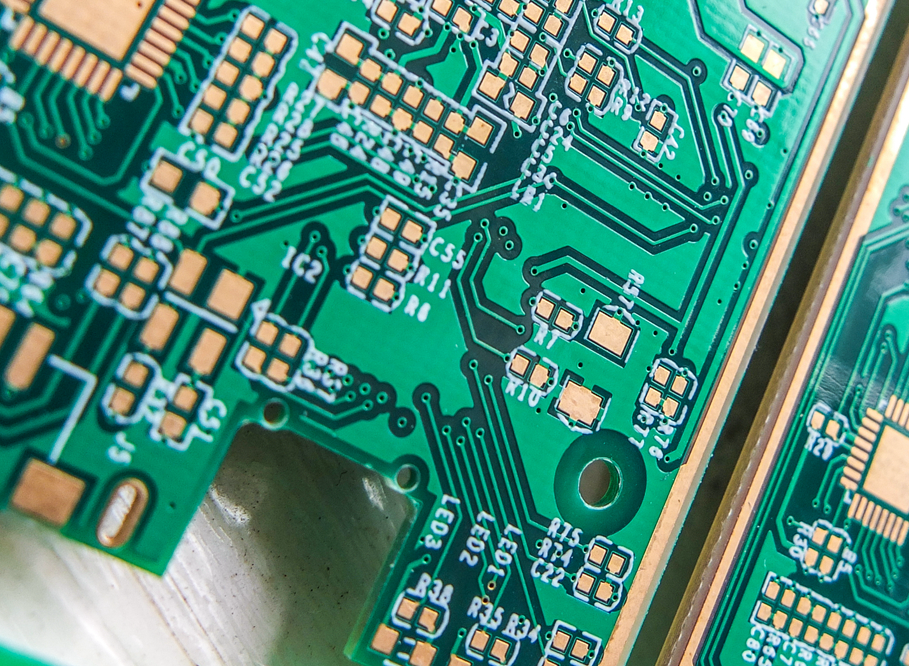


Just upload Gerber files, BOM files and design files, and the KINGFORD team will provide a complete quotation within 24h.