
Professional PCB manufacturing and assembly
Building 6, Zone 3, Yuekang Road,Bao'an District, Shenzhen, China
+86-13410863085Mon.-Sat.08:00-20:00

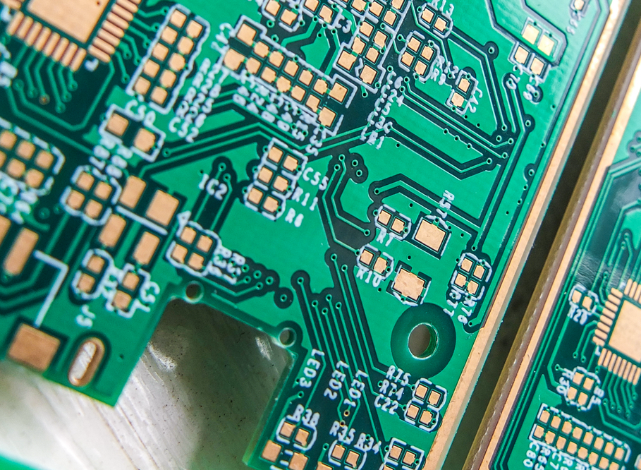
PCB Assembly
In our ongoing series describing the more common problems associated with printed circuit boards, we examine design, assembly, and manufacturing issues. Next, we'll focus on some issues that can affect the board during assembly. While some of these problems may be caused by manufacturing errors, the root of most problems lies in the way the board was designed. These issues can range from minor annoyances such as unmarked polarity indicators to production demonstration hindrances such as missing components in the bill of materials.
Often, design for manufacturability (DFM) issues stem from PCB layout, but do not receive the attention they deserve. When this happens, it is the manufacturer's responsibility to find the error, go back to the design for corrections, or make the changes themselves. This situation could turn into an expensive and time-consuming process that could have been avoided if the design team had prepared adequately early on. To help identify these potential issues and ensure your PCB design is production-ready before sending it out, here are some common printed circuit board issues you should know about in assembly.
Eight Common PCB Assembly Problems
Many board problems during assembly are due to design and layout issues that the designer is not aware of. Below are eight common issues that can slow or stop PCB manufacturing.
1. Bill of Materials (BOM) issues
Your PCB contract manufacturer will review your BOM before starting your project, they will look for the following:
Component Availability: Some parts are out of stock or no longer in production.
Price: In some cases, the part you want is expensive, and a functional replacement may be much less expensive.
Fakes: Some parts are not as advertised, but CM staff are trained to spot these fakes and avoid them.
Supply Chain: PCB CM has a well-established network of component manufacturers, distributors and brokers that they can leverage to solve many of the challenges in today's supply chain.
You can avoid delays caused by BOM issues by working with your CM early in the design cycle so they have the part ready when you are ready for manufacturing.
2. Incorrect PCB footprint
If built incorrectly, PCB footprints can create several DFM issues, including poor solder joints, mismatched pins, or lack of physical space. Industry or manufacturing specifications must be used when constructing CAD package models and ensuring that they correctly match the part numbers in the schematic.
3. Component placement errors
Components that are too close together to violate a manufacturer's DFM rules can cause difficulties for automated assembly systems. Pick and place machines as well as wave and reflow soldering require minimal spacing for best results. Manual rework also requires adequate component spacing. It can be challenging to get a soldering iron into one area when the component is hidden by another larger part. There is also a risk of collateral damage to nearby components attempting to fit the tool into tight spaces.
4. Welding defects
Violation of DFM rules can also produce various soldering defects in printed circuit boards. The following are examples of what might happen:
Solder Bridging: When solder creates a connection or short circuit between two metal conductors that were not intended to be connected, it is called a solder bridge. This defect can occur if the component is wave soldered incorrectly, if the solder mask design is incorrect resulting in excess solder on the pad, or if there is a design or alignment issue with the solder stencil.
Shading: Larger parts putting smaller parts into wave soldering can shadow the smaller parts and rob them of the solder they need to make a good connection.
Bad solder joints: In through-hole components, this is usually due to insufficient thermal pads leading to too much heat being carried away from the connection during soldering.
Tombstoning: In small two-pin surface mount parts, too much metal on one pin can create a thermal imbalance that causes the solder on the other pin to melt faster and pulls the part away from the cooler pin Pull up and down.
Dented joints: Through-hole pins that are too large for their pins may not hold as much molten solder as they should, resulting in an incomplete connection.
5. Thermal issues
Boards with asymmetrical stackups can warp and twist due to the heat applied during soldering operations. These same thermal issues can also adversely affect heat-sensitive components that need to be manually assembled later.
6. Lack of testability
PCB manufacturers use board testing to verify the assembly process, ensuring that each component pin has a good connection to its associated net. Without complete coverage of the test points placed according to the Design for Test (DFT) rules, the test cannot be fully completed and requires a manual verification process.
7. Insufficient Silkscreen Marking
Accurate silkscreen markings such as reference designators and polarity indicators are critical for assembly verification, rework and testing. Without these markings, test technicians would have the more time-consuming and challenging job of finding the right spot on the board to work on.
8. Incomplete or unclear assembly documentation
Assembly documentation needs to be complete and up to date for the board being built. Drawings need to be readable and all required data and information files need to accompany the design for manufacture.


Just upload Gerber files, BOM files and design files, and the KINGFORD team will provide a complete quotation within 24h.