
Professional PCB manufacturing and assembly
Building 6, Zone 3, Yuekang Road,Bao'an District, Shenzhen, China
+86-13410863085Mon.-Sat.08:00-20:00


The specific steps and composition of printed circuit board (PCB)
With the improvement of microelectronics technology and industrial manufacturing level, printed circuit board (PCB) has become the basic unit of all smart devices and systems. PCB can realize the wiring and electrical connection or electrical connection between various electronic components such as integrated circuits. Insulation, providing the required electrical characteristics, providing solder mask graphics for automatic welding, and providing identification characters and graphics for component insertion, inspection, and maintenance.
1. The general steps of PCB
The design of the printed circuit board is based on the circuit schematic diagram to realize the functions required by the circuit user. The design of the printed circuit board mainly refers to the layout design, which requires the layout of internal electronic components, metal wiring, through holes and external connections. , point protection, heat dissipation, crosstalk and other factors, excellent circuit design can save production cost, achieve good circuit performance and heat dissipation performance, simple layout design can be realized by hand, but complex circuit design is generally not It needs to be realized with the help of computer aided design (CAD).
Famous design software includes OrCAD, Pads (ie PowerPCB), Altium Designer, FreePCB, CAM3501, etc. When designing circuit boards, first of all, the pin size and structure package form of all components in electronic production should be marked with detailed and real specific numbers. It should be noted that sometimes the perineal manufacturers of the same type of components have different values and pin arrangements;
Secondly, according to the designed electrical schematic diagram, simulate the overall block diagram of the components; finally, according to the block diagram and electrical requirements, in the sketch of the circuit board, when drawing the detailed pins of each component and their positions on the circuit board, care should be taken The size of components and the distance between them, the size of peripheral components from the edge, input and output, grounding and power lines, high-frequency circuits, signal lines that are prone to radiation and interference, etc.
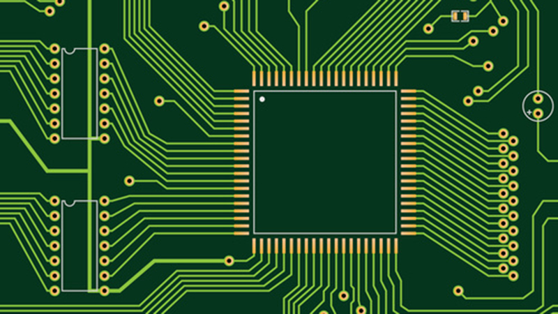
2. Composition of PCB
1) Line and drawing (Pttern): The line is used as a tool for the conduction between the original components. In the design, a large copper surface is additionally designed as the grounding and power layer. The line and the drawing are made at the same time.
2) Dielectric layer (Dielectric): It is used to maintain the insulation between lines and layers, commonly known as the substrate.
3) Trough hole/via: The via hole can make the lines of more than two levels conduct each other, the larger via hole is used as a component plug-in, and the non-conducting hole (nPTH) is usually used as a Surface mount positioning, used for fixing screws during assembly.
4) Solder resist ink (Soldcr resistant/Solder Mask): Not all copper surfaces have to eat tin parts, so the non-tin-eaten area will be printed with a layer of material (usually epoxy resin) that isolates the copper surface from eating tin , Avoid short circuit between non-tin-eaten lines. According to different processes, it is divided into green oil, red oil and blue oil.
5) Silk screen (Legend /Marking/Silk screen): This is a non-essential component. Its main function is to mark the name and position box of each part on the circuit board, which is convenient for maintenance and identification after assembly.
6) Surface Finish: Since the copper surface is easily oxidized in the general environment, it cannot be tinned (poor solderability), so it will be protected on the copper surface that eats tin. The protection methods include HASL, ENIG, Imersion Silver, Imersion Tin, and OSP. Each method has its advantages and disadvantages, and they are collectively referred to as surface treatment.
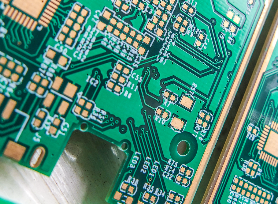
The production process of PCB is relatively complicated, and it involves a wide range of processes, from simple mechanical processing to complex mechanical processing, common chemical reactions, photochemical, electrochemical, thermochemical and other processes, computer-aided design CAM and other knowledge . Moreover, there are many technological problems in the production process and new problems will be encountered from time to time, and some problems will disappear without finding out the cause. Since the production process is a discontinuous assembly line, any problem in any link will cause the entire line to stop production Or the consequences of a large number of scrapping. If the printed circuit board is scrapped, it cannot be recycled and reused. The work pressure of process engineers is relatively high, so many engineers leave this industry and go to printed circuit board equipment or material suppliers to do sales and technical services. .
The substrate of the board itself is made of insulating and heat-insulating material that is not easy to bend. The small circuit material that can be seen on the surface is copper foil. Originally, the copper foil covered the entire board, but in the manufacturing process part It is etched away, and the remaining part becomes a network of fine lines. These lines are called conductors.
pattern) or wiring, and is used to provide circuit connections for parts on the PCB.
In order to fix the parts on the PCB, we solder their pins directly to the wiring. On the most basic PCB (single panel), the parts are concentrated on one side, and the wires are concentrated on the other side. In this way we It is necessary to make holes on the board so that the pins can pass through the board to the other side, so the pins of the parts are soldered on the other side. Because of this, the front and back sides of the PCB are called the component side (Component
Side) and welding surface (Solder Side).
If there are some parts on the PCB that need to be removed or put back after the production is completed, then the socket (Socket) will be used when installing the part. Since the socket is directly welded on the board, the parts can be disassembled and assembled arbitrarily .
If two PCBs are to be connected to each other, we generally use edge joints commonly known as "golden fingers".
connector). The gold finger contains many exposed copper pads, which are actually part of the PCB wiring. Usually, when connecting, we insert the gold finger on one of the PCBs into the appropriate slot on the other PCB (Generally called the expansion slot Slot). In the computer, such as a display card, sound card or other similar interface cards, are connected to the motherboard by golden fingers.
The green or brown on the PCB is the solder resist paint (solder
The color of the mask). This layer is an insulating protective layer that can protect the copper wire and prevent parts from being soldered to incorrect places. A layer of silk screen printing (silk) will be printed on the solder mask
screen). Usually, text and symbols (mostly white) are printed on it to mark the position of each part on the board. The screen printing surface is also called the icon surface (legend).
The printed circuit board etches the complex circuit copper wires between parts and parts on a board after careful and neat planning, providing the main support for electronic components during installation and interconnection, and is indispensable for all electronic products basic parts.
A printed circuit board is a flat plate made of non-conductive material, on which there are usually pre-drilled holes designed to install chips and other electronic components. The holes of the components help to electronically connect the pre-defined metal paths printed on the board. After the pins of the electronic components pass through the PCB, they are then adhered to the PCB with conductive metal welding rods to form a circuit.
PCB assembly in the medical industry
Jun 02,2023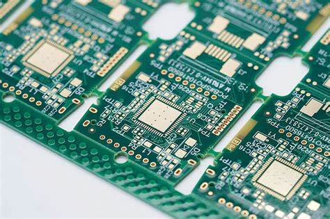


Just upload Gerber files, BOM files and design files, and the KINGFORD team will provide a complete quotation within 24h.