
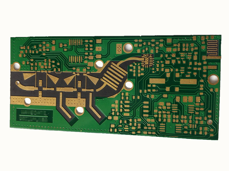
Professional PCB manufacturing and assembly
Building 6, Zone 3, Yuekang Road,Bao'an District, Shenzhen, China
+86-13410863085Mon.-Sat.08:00-20:00

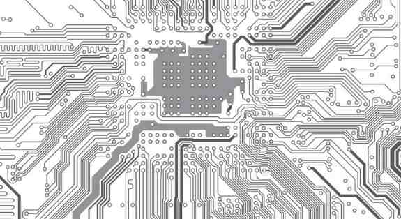
Chemically etched SMT patch processing templates are the international premier type of templates. They have the lowest cost and the fastest turnover. Chemically etched stainless steel stencils are manufactured by applying an anti-corrosion protector to the foil, exposing the figure on both sides of the foil with a pin to position the sensitive object, and then using a double-sided technique to corrode the foil from both sides.
Because the skill is double-sided, corrosives through the holes, or openings, that occur in the metal, not only from the top and bottom surfaces, but also horizontally. Inherent in this skill is the shape of a blade, or hourglass. This shape has a blocking moment at distances below 0.020 ", and this flaw can be reduced using an enhanced skill called electropolishing.
Chemical etching refers to a technology that removes materials through chemical reaction or physical impact. etching technology can be divided into "wet etching" and "dry etching".
Generally referred to as etching, also known as photochemical etching, it refers to the removal of the protective film in the etched area through exposure platemaking and development, and contact with chemical solution during etching to achieve the role of dissolution corrosion, resulting in the formation of concave and convex or hollow molding.
SMT SMT can be used to manufacture copper plate, zinc plate and other printing concave and convex plate, is also widely used in Weight Reduction instrument panel, famous brand and traditional processing method is difficult to process thin workpiece. After continuous improvement and development of process equipment, it can also be used for precision etching products of electronic wafer parts in aviation, machinery, chemical industry, especially in the semiconductor process, etching is an indispensable technology. For example, Moto V3 keyboard, text and symbols are hollow etching process.
The cause and control method of SMT welding pore formation
Pore formation is often a problem associated with welded joints. Especially the application of SMT technology to soft fusion solder paste, in the use of leadless ceramic chip, most of the large pores (> 0.0005 inch /0.01 mm) is between the LCCC solder joint and the PCB solder joint. Meanwhile, there are only a few small pores in the fillet welds near the LCCC castle, The existence of pores will affect the mechanical properties of welded joints and damage the strength, ductility and fatigue life of joints. This is because the growth of pores converges into extendable cracks and leads to fatigue. Pores will also increase the stress and covariant of solder, which is also a tableland cause for damage. In addition, the solder will shrink during solidification, and the stratified exhaust and flux entrain during welding electroplating through holes are also the cause of porosity.
In the welding process, the mechanical system of forming pores is more complicated, Generally speaking, the porosity is caused by the flux exhaust in the solder in the sandwich structure during soft melting. (2,13) the formation of pores is mainly determined by the weldability of the metallized zone, and changes with the decrease of the flux activity, the increase of the metal load of the powder and the increase of the covering area under the lead joint. Reducing the size of the solder particles can only increase the porosity. In addition, pore formation is related to the allocation of time between the coalescence of solder powder and the elimination of fixed metal oxides. The earlier the solder paste coalesces, the more pores are formed. In general, the proportion of macropores increases with the total pore volume. Those suggestive pore-forming factors will have a greater impact on the reliability of welded joints than the results of the total porosity analysis indicate.
Methods of controlling pore formation include:
1, improve the solderability of components/shirt bottom;
2, the use of high welding activity of the flux;
3, reduce the powder oxide of solder;
4, the inert heating atmosphere.
5. Slow down the preheating process before soft melting.
In contrast, pore formation in BGA assembly follows a slightly different pattern (14). In general, in BGA assembly with tin 63 solder blocks, pores are mainly formed at the plate stage of assembly. On pre-tinned PCB, the porosity of BGA joint increases with the increase of solvent volatility, metal composition and melting temperature, and also with the decrease of powder size. This is explained by the viscosity which determines the flux discharge rate. According to this model, flux media with higher viscosity at soft melt temperatures will prevent flux from escaping from the molten solder, so increasing the amount of entraining flux will increase the likelihood of outgassing, resulting in greater porosity in the BGA assembly.
Without considering the solderability of the fixed metallization zone, the effect of flux activity and soft melting atmosphere on pore formation appears to be negligible. The proportion of macropores increases with the total porosity, indicating that the factors causing pore formation in BGA have a greater impact on the reliability of welded joints than indicated by the total porosity analysis, which is similar to the case of void formation in SMT.
V-CUT process problem of PCB board
May 30,2023


Just upload Gerber files, BOM files and design files, and the KINGFORD team will provide a complete quotation within 24h.