
Professional PCB manufacturing and assembly
Building 6, Zone 3, Yuekang Road,Bao'an District, Shenzhen, China
+86-13410863085Mon.-Sat.08:00-20:00

Advantages of SMT chip processing technology
With the continuous progress and development of the electronic industry, SMT surface mounting technology has become increasingly mature, and equipment functions have been continuously improved SMT chip processing This technology has gradually replaced the traditional ink cartridge technology and has become the most popular technology in the electronic assembly industry "Smaller, lighter, higher density, and" better "are SMT chip processing technologies, which are also the requirements for highly integrated and miniaturized electronic products
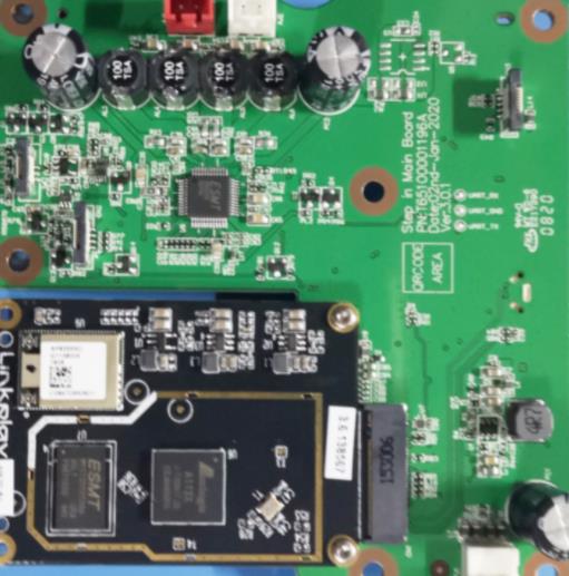
SMT chip processing process: first, paint solder paste on the surface of PCB pad, then accurately place the metallized terminal or pin of the component on the solder paste of the pad, then connect the PCB to the component, put it into the reflow furnace, and heat the whole to melt the solder paste. After the solder paste is cooled and solidified, the mechanical and electrical connection between the components and the printed circuit is realized. As a professional SMT chip processing factory, Lingxinte can provide users with various SMT services such as SMT processing rapid proofing, difficult to process SMT chips, and special SMT chip processing. Let's take a look at the advantages of SMT chip processing technology:
The volume of SMT chip modules is only about 1/10 of the traditional chip modules, and the weight is only 10% of the traditional chip modules In general, the use of surface mount technology can reduce the volume of electronic products by 40% - 60%, the quality by 60% - 80%, and the floor area and weight by a large margin The SMT patch processing assembly component grid has developed from 1. 27MM to 0.63MM, and the single grid has reached 0.5mm Through hole installation technology is used to install components, which can make the assembly density higher
2. High reliability and strong anti vibration capability
SMT chip processing uses highly reliable chip components. The component has small volume, light weight and strong anti vibration ability. Automatic production is adopted, with high installation reliability. Generally, the rate of defective solder joints is less than 10 parts per million. The wave soldering technology of through hole plug-in components is one order of magnitude lower than the traditional wave soldering technology, which can ensure that the solder joint defect rate of electronic products or components is low. At present, nearly 90% of electronic products use SMT technology.
3. High frequency characteristic, reliable performance
Because the chip modules are firmly installed, the devices are usually lead-free or short leads, which reduces the impact of parasitic inductance and capacitance, improves the high-frequency characteristics of the circuit, and reduces electromagnetic and radio frequency interference. The maximum frequency of the circuit designed with SMC and SMD is 3GHz, while the chip module is only 500MHz, which can shorten the transmission delay time. It can be used in circuits with clock frequency higher than 16MHz. If MCM technology is used, the high-end clock frequency of computer workstation can reach 100MHz, and the additional power consumption caused by parasitic reactance can be reduced by 2-3 times.
4. Improve production efficiency and realize automatic production
At present, if the perforated printed circuit board is to be fully automated, the area of the original printed circuit board needs to be expanded by 40% so that the insertion head of the automatic part can be inserted into the component, otherwise the space is insufficient and the part will be damaged. The automatic placement machine (SM421/SM411) uses a vacuum nozzle to pick and place components. The vacuum nozzle is smaller than the shape of the component, which increases the installation density. In fact, small parts and fine pitch QFP equipment are produced by automatic placement machine to realize automatic production of the whole line.
5. Reduce costs and expenses
(1) The use area of printed board is reduced, which is 1/12 of that of through-hole technology. If CSP is used for installation, its area will be greatly reduced;
(2) The number of holes drilled on the printed circuit board is reduced, and the maintenance cost is saved;
(3) Due to the improvement of frequency characteristics, the cost of circuit debugging is reduced;
(4) Due to the small size and light weight of the chip module, the packaging, transportation and storage costs are reduced;
Using SMT chip processing technology can save data, energy, equipment, labor, time, etc, And it can reduce the cost by 30% - 50%
With the continuous progress and development of the electronic industry, SMT surface mounting technology has become increasingly mature, and equipment functions have been continuously improved SMT chip processing This technology has gradually replaced the traditional ink cartridge technology and has become the most popular technology in the electronic assembly industry "Smaller, lighter, higher density, and" better "are SMT chip processing technologies, which are also the requirements for highly integrated and miniaturized electronic products
SMT chip processing process: first, paint solder paste on the surface of PCB pad, then accurately place the metallized terminal or pin of the component on the solder paste of the pad, then connect the PCB to the component, put it into the reflow furnace, and heat the whole to melt the solder paste. After the solder paste is cooled and solidified, the mechanical and electrical connection between the components and the printed circuit is realized. As a professional SMT chip processing factory, Lingxinte can provide users with various SMT services such as SMT processing rapid proofing, difficult to process SMT chips, and special SMT chip processing. Let's take a look at the advantages of SMT chip processing technology:
The volume of SMT chip modules is only about 1/10 of the traditional chip modules, and the weight is only 10% of the traditional chip modules In general, the use of surface mount technology can reduce the volume of electronic products by 40% - 60%, the quality by 60% - 80%, and the floor area and weight by a large margin The SMT patch processing assembly component grid has developed from 1. 27MM to 0.63MM, and the single grid has reached 0.5mm Through hole installation technology is used to install components, which can make the assembly density higher
2. High reliability and strong anti vibration capability
SMT chip processing uses highly reliable chip components. The component has small volume, light weight and strong anti vibration ability. Automatic production is adopted, with high installation reliability. Generally, the rate of defective solder joints is less than 10 parts per million. The wave soldering technology of through hole plug-in components is one order of magnitude lower than the traditional wave soldering technology, which can ensure that the solder joint defect rate of electronic products or components is low. At present, nearly 90% of electronic products use SMT technology.
3. High frequency characteristic, reliable performance
Because the chip modules are firmly installed, the devices are usually lead-free or short leads, which reduces the impact of parasitic inductance and capacitance, improves the high-frequency characteristics of the circuit, and reduces electromagnetic and radio frequency interference. The maximum frequency of the circuit designed with SMC and SMD is 3GHz, while the chip module is only 500MHz, which can shorten the transmission delay time. It can be used in circuits with clock frequency higher than 16MHz. If MCM technology is used, the high-end clock frequency of computer workstation can reach 100MHz, and the additional power consumption caused by parasitic reactance can be reduced by 2-3 times.
4. Improve production efficiency and realize automatic production
At present, if the perforated printed circuit board is to be fully automated, the area of the original printed circuit board needs to be expanded by 40% so that the insertion head of the automatic part can be inserted into the component, otherwise the space is insufficient and the part will be damaged. The automatic placement machine (SM421/SM411) uses a vacuum nozzle to pick and place components. The vacuum nozzle is smaller than the shape of the component, which increases the installation density. In fact, small parts and fine pitch QFP equipment are produced by automatic placement machine to realize automatic production of the whole line.
5. Reduce costs and expenses
(1) The use area of printed board is reduced, which is 1/12 of that of through-hole technology. If CSP is used for installation, its area will be greatly reduced;
(2) The number of holes drilled on the printed circuit board is reduced, and the maintenance cost is saved;
(3) Due to the improvement of frequency characteristics, the cost of circuit debugging is reduced;
(4) Due to the small size and light weight of the chip module, the packaging, transportation and storage costs are reduced;
Using SMT chip processing technology can save data, energy, equipment, labor, time, etc, And it can reduce the cost by 30% - 50%

On Selective Wave Soldering in PCB Manufacturing
Dec 04,2022


Just upload Gerber files, BOM files and design files, and the KINGFORD team will provide a complete quotation within 24h.