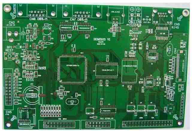
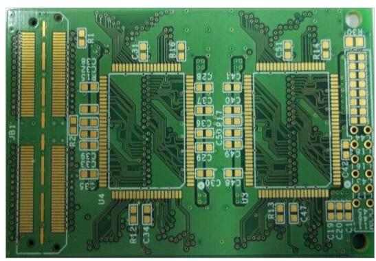
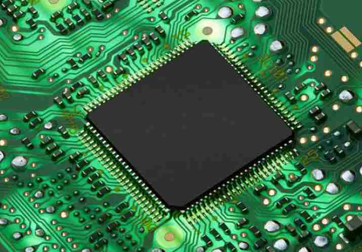
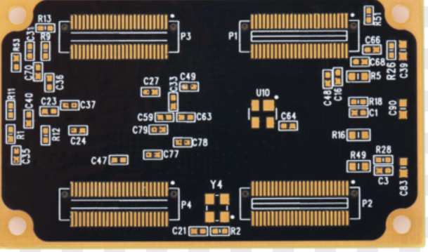
Five requirements for PCB processing
The size of PCB is limited by the capability of the equipment in the electronic processing line, the...

The size of PCB is limited by the capability of the equipment in the electronic processing line, the...
The layout should meet the following requirements as far as possible: the overall connection should ...
The design of high frequency circuit PCB is a complicated process, which involves many factors, whic...
Wiring is the general requirement of high frequency PCB design on the basis of reasonable layout. Wi...
Both schematic drawing and PCB design should be considered from the high frequency working environme...
In SMT processing, it is often necessary to replace chip components. When replacing chip components,...
Many friends do not know how to charge for SMT processing. kingford SMT processing charge details ar...
Every hole on PCB is called through hole. From the perspective of function, through hole can be divi...
The manufacturing process of PCBA involves many links, and only by controlling the quality of each l...
Then use these technical documents and production documents to make PCB board, component welding, fl...
It's best to take two pictures of the device's location with a digital camera. A lot of pcb circuit ...
The signal integrity problems of PCB mainly include signal reflection, crosstalk, signal delay and t...
