
Professional PCB manufacturing and assembly
Building 6, Zone 3, Yuekang Road,Bao'an District, Shenzhen, China
+86-13410863085Mon.-Sat.08:00-20:00

How to control the quality of PCBA proceKingFord is a PCBA OEM manufacturer that provides PCB circuit board manufacturing, component purchasing, SMT patch processing, DIP plug-in processing and PCBA testing one-stop services. Next, we will introduce how to control the quality of PCBA processing. The manufacturing process of PCBA involves many links, and the quality of each link must be well controlled to produce good products. Generally, PCBA is composed of: PCB circuit board manufacturing, component procurement and inspection, SMT patch processing, plug-in processing, program firing, testing, aging and a series of processes, the following we carefully explain the need to pay attention to each link.
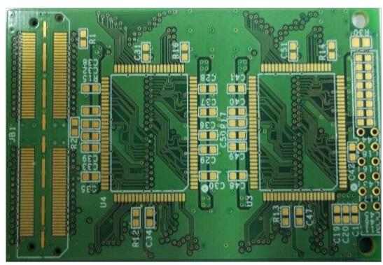
1, PCB circuit board manufacturing received PCBA orders, analysis of Gerber files, pay attention to the PCB hole spacing and the bearing capacity of the plate, do not cause bending or fracture, wiring whether to take into account high frequency signal interference, impedance and other key factors.
2. The procurement and inspection of components and components need to strictly control the channels, be sure to pick up goods from large traders and original factories, and avoid second-hand materials and fake materials 100%. In addition, set up a special incoming material inspection post, strict inspection of the following items, to ensure that components without fault. PCB: reflow furnace temperature test, no fly line, whether hole plugging or leakage ink, board surface bending, etc.; IC: Check whether the silk screen is consistent with BOM, and store it at constant temperature and humidity; Other common materials: check silkscreen, appearance, power measurement, etc. Check items are carried out in the way of random inspection, and the proportion is generally 1-3%.
3, SMT Assembly processing solder paste printing and reflow furnace temperature control is the key points, it is very important to use good quality and meet the process requirements of laser steel mesh. According to the requirements of PCB, part of the steel mesh should be enlarged or reduced, or U-shaped holes should be used to make steel mesh according to the technological requirements. The furnace temperature and speed control of reflow welding is very critical for solder paste infiltration and welding reliability, which can be controlled according to normal SOP operating guidelines. In addition, strict implementation of AOI testing is required to minimize adverse human factors.
4. DIP plug-in processing plug-in technology, the mold design of over-wave soldering is the key point. How to use the mold to maximize the probability of good products after furnace is a process that PE engineers must constantly practice and summarize experience.
5. Program firing In the early DFM report, it is suggested to the customer to set some Test Points on the PCB for the purpose of testing the PCB and PCBA circuit connectivity after all components are soldered. If conditions, you can ask the customer to provide the program, through the burner (such as ST-LINK, J-LINK, etc.) will be fired into the main control IC, you can be more intuitive test a variety of touch action brought by the functional changes, in order to test the functional integrity of the whole block of PCBA.
6. PCBA board Test For orders with PCBA Test requirements, the main Test contents include ICT(In Circuit Test), FCT(Function Test), Burn In Test(aging test), temperature and humidity test, drop test, etc. Operate according to the customer's test plan and summarize the report data.

How do engineers plan circuit board designs
I. Planning of power supply and stratum number
The number of layers of power supply is mainly determined by the number of power supply types, distribution, current carrying capacity, performance indicators of the board and the cost of the board. Two conditions must be met for setting the power plane: The power supplies are not interconnected; Avoid adjacent layers of important signals across segmentation. The following points should be paid attention to in the setting of the number of layers of the ground: the second layer of the main device should have a relatively complete ground plane; High speed, high frequency, clock and other important signals should refer to the ground plane; The main power supply is tightly coupled to the ground plane, reducing the impedance of the power plane and so on.
Ii. Signal layer number planning
The routing channel is usually an important factor in determining the number of signal layers. First of all, it should be clear whether there is a deep BGA and connector on the board. The depth of the BGA and the PIN spacing of the BGA are the key to determine the number of BGA lines. For example, two lines can be passed between 1.0mm BGA holes, and only one line can be passed between 0.8mm BGA holes. There is a great difference between the two lines. The connector mainly considers its depth, basically two holes between a pair of difference lines. The BGA outlet that can pass two wires between two holes and share two wiring layers. The BGA outlet that can only pass one wire between two holes and share four wiring layers should also consider the wiring channel of high-speed signals on the board. Because there are more requirements for high-speed signal processing, factors such as stub, distance between cables and reference plane should be considered. Therefore, it is necessary to consider whether the wiring channel is sufficient.
The last is the planning of the bottleneck area. After the basic layout is handled well, it is necessary to focus on the relatively narrow bottleneck area. Considering the difference line, sensitive signal line, special signal topology, etc., the maximum number of lines can be calculated in the bottleneck area and the number of layers to allow all the required lines to pass through this area. Taking the above two points into consideration, there is basically no part of the line can not go through, someone said metaphorically: is like a process of building pcb designall buildings, wiring layer planning is one of the design drawings, planning, wiring will naturally come naturally.
How to design holes in PCB wiring
Feb 03,2023


Just upload Gerber files, BOM files and design files, and the KINGFORD team will provide a complete quotation within 24h.