
Professional PCB manufacturing and assembly
Building 6, Zone 3, Yuekang Road,Bao'an District, Shenzhen, China
+86-13410863085Mon.-Sat.08:00-20:00

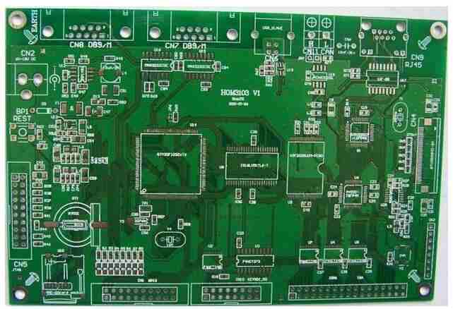
1.kingford is a PCB wiring design company with excellent design experience PCB design engineer team, can provide multi-layer, high frequency, high speed PCB wiring design services. Next, how to design holes in PCB wiring? What is a hole? Through hole (via) is one of the important components of multilayer PCB, the cost of drilling usually accounts for 30% to 40% of the PCB board. Simply put, every hole in the PCB can be called a pass hole.
From the point of view of function, the hole can be divided into two categories: one is used as an electrical connection between the layers; The second is used for fixing or positioning devices. If from the process, through the hole is generally divided into three categories, namely blind hole, buried hole and through hole. Blind holes are located on the top and bottom surfaces of the PCB and are of a certain depth. They are used to connect the surface circuit to the inner circuit below. The depth of the holes usually does not exceed a certain ratio (aperture). Buried holes are connection holes located in the inner layer of the PCB that do not extend to the surface of the PCB. Both types of holes are located in the inner layer of the circuit board, which is completed by a through-hole molding process prior to lamination. Several inner layers may be overlapped during the through-hole formation process. The third type, called through-holes, runs through the entire circuit board and can be used for internal interconnection or as installation positioning holes for components. Because the through hole in the process is easier to achieve, the cost is lower, so most of the printed circuit board is used in it, rather than the other two through holes.
The following mentioned through holes, without special instructions, are considered as through holes. From the design point of view, a hole is mainly composed of two parts, one is the middle of the drilling hole, the other is the welding pad area around the drilling hole. The size of these two parts determines the size of the hole. Obviously, in the design of high speed, high density PCB, the designer always wants the hole as small as possible, the template can leave more wiring space, in addition, the hole is smaller, its own parasitic capacitance is smaller, more suitable for high speed circuit. However, the decrease of hole size also brings the increase of cost, and the size of the hole can not be reduced indefinitely, it is limited by drilling and electroplating technology: the smaller the hole, the longer the drilling time, and the more easy to deviate from the center position; When the hole depth is more than 6 times the diameter of the hole, it is impossible to guarantee the uniform copper plating on the hole wall. For example, the thickness (through hole depth) of a normal 6-layer PCB board is about 50Mil, so the minimum drilling diameter provided by PCB manufacturers can only reach 8Mil. Parasitic properties of pores.

2. How to select PCB board correctly
With the rapid development of digital systems, the problem of transmission line loss, which was previously considered insignificant, is now becoming the primary concern of PCB design. When the clock frequency is higher than 1GHz, the impact of frequency-dependent transmission loss has actually occurred, especially in the high-speed SerDes interface. The signal has a very fast rise time, and the digital signal can carry the energy of higher frequency than its own repetition frequency. These high frequency energy components are used to construct the ideal digital signal of rapid conversion. Today's high-speed serial buses tend to have a large concentration of energy on the fifth harmonic of the clock rate. There are many high speed digital applications available today with speeds of 10 Gbit/s or higher. These applications use a 5 GHz fundamental frequency and harmonics of 15 GHz, 25 GHz, etc. Most common PCB materials in this frequency range will vary significantly in terms of dielectric loss (Df) and cause serious signal integrity problems. This is one of the reasons high speed digital PCBS use special boards designed for high frequency applications.
These materials are formulated with a low loss factor and minimal variation over a wide range of frequencies. These plates used to be used for high frequency RF applications and are even now used for 77 GHz and higher applications. In addition to the improved dielectric loss factor, these panels are equipped with strict thickness and Dk controls to ensure signal integrity. In Computex 2019, AMD announced the third-generation Ryzen processor. In addition to the performance of the 7nm CPU, AMD began to beat Intel. Its supporting X570 chipset also introduced PCIe 4.0 support, and SSDS using PCIe 4.0 NVMe began to be introduced to the market. The PCIe 5.0 specification is expected to be released in two years.
PCIe 5.0's data rate will reach a terrifying 32GT/s, exacerbating frequency-related insertion losses. The PCB material chosen can have a huge impact on the insertion loss in each area. If PCBS are designed without considering the impact of the board on high-speed signals, older drivers can flip over too! When selecting PCB board, it is necessary to strike a balance between meeting PCB design requirements, mass production and cost. In short, the design requirements include both electrical and structural reliability. The board issue is usually important when designing very high speed PCB boards (frequencies greater than GHz).
For example, the FR-4 material commonly used now has a high dielectric loss Df (Dielectricloss) at several GHz frequencies and may not be suitable. The running speed of high speed digital circuit is the main factor considered in PCB selection. The higher the circuit speed, the smaller the Df value of the selected PCB should be. With medium, low loss circuit board will be suitable for 10Gb/S digital circuit; 25Gb/s digital circuit is suitable for plates with lower losses; The ultra-low loss sheet will accommodate faster, high-speed digital circuits at speeds of 50Gb/s or more.
PCB layout method tips
Feb 03,2023


Just upload Gerber files, BOM files and design files, and the KINGFORD team will provide a complete quotation within 24h.