
Professional PCB manufacturing and assembly
Building 6, Zone 3, Yuekang Road,Bao'an District, Shenzhen, China
+86-13410863085Mon.-Sat.08:00-20:00


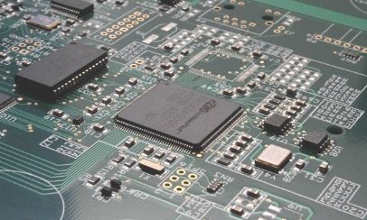
1. Pad and aperture
The pads should be designed to be large enough to ensure adequate ring width, provided that the minimum wiring spacing does not violate the PCB designed electrical spacing. Generally, the inner hole of the pad is slightly larger than the lead diameter of the components, and the design is too large, which is easy to form virtual welding in welding. The outer diameter D of the pad is generally no less than (d+1.2)mm, where d is the inner aperture of the pad. For some PCB board with relatively high density, the minimum value of the pad can be (d+1.0) mm. The shape of the pad is usually set as a circle, but it is best to use the racetrack shape of the pad for DIP-packaged IC, which can increase the area of the pad in the limited space, which is conducive to the welding of IC. The connection between wiring and pad should be smooth transition, that is, when the width of wiring into the round pad is smaller than the diameter of the round pad, the teardrop design should be adopted.
It should be noted that the size of the aperture d in the pad is different, and should be considered according to the size of the actual lead diameter of the components, such as component holes, mounting holes and slot holes. And the hole distance of the pad should also be considered according to the actual installation mode of the components, such as resistance, diode, tubular capacitor and other components have "vertical" and "horizontal" installation mode, the hole distance of the two ways is different. In addition, the design of pad hole spacing should also consider the minimum clearance requirements between components, especially the gap between special components need to be guaranteed by the hole spacing between the pads.
In high frequency PCBS, the number of holes should also be minimized to reduce the distributed capacitance and increase the mechanical strength of the PCB. In short, in the design of high frequency PCB, the design of pad and its shape, aperture and hole spacing should not only consider its particularity, but also meet the requirements of production technology. Adopting standardized design can not only reduce product cost, but also improve production efficiency while ensuring product quality.
2. Apply copper
The main purpose of copper coating is to improve the anti-interference ability of the circuit, at the same time for PCB heat dissipation and printed circuit board strength has great benefits, copper grounding can play a shielding role. But can not use a large area of strip copper foil, because in the use of PCB for too long will produce large heat, at this time strip copper foil prone to expansion and fall off phenomenon, therefore, in the copper is best to use grid copper foil, and the grid and the grounding network of the circuit is connected, so that the grid will have a better shielding effect, the size of the grid grid by the shielding frequency The rate depends.
DRC(Design Rule check) should be performed after the wiring, pad and hole design is completed. The differences between the designed graph and the defined rules are detailed in the inspection results, which can identify the network that does not meet the requirements. However, DRC should be run only after parameters are set before wiring, that is, by executing the ToolsDesign Rule Check command.
The design of high frequency circuit PCB is a complicated process, which involves many factors, which may directly affect the performance of high frequency circuit. Therefore, designers need to continue to study and explore in the actual work, accumulate experience, and combined with the new EDA (electronic design automation) technology in order to design high frequency circuit PCB with excellent performance.
Some specification requirements for PCB design
Feb 03,2023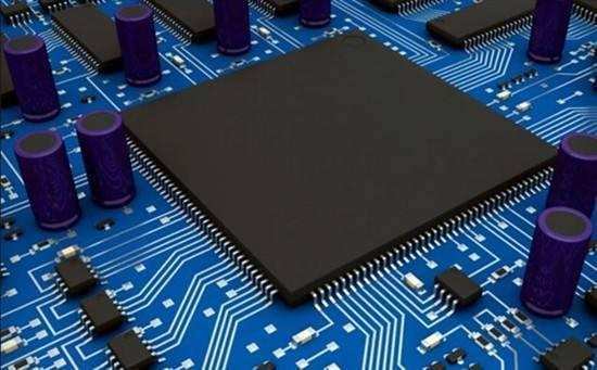


Just upload Gerber files, BOM files and design files, and the KINGFORD team will provide a complete quotation within 24h.