
Professional PCB manufacturing and assembly
Building 6, Zone 3, Yuekang Road,Bao'an District, Shenzhen, China
+86-13410863085Mon.-Sat.08:00-20:00

Wiring design
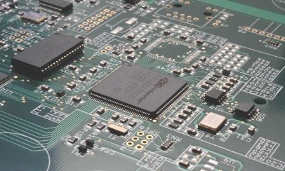
Wiring is the general requirement of high frequency PCB design on the basis of reasonable layout. Wiring includes automatic wiring and manual wiring. Usually, no matter how many key signal lines there are, these signal lines are first routed manually. After the wiring is completed, the wiring of these signal lines is carefully checked. After the check is passed, the signal lines are fixed, and then other wiring is automatically routed. That is, the combination of manual and automatic wiring is used to complete PCB wiring.
In the wiring process of high frequency PCB should pay special attention to the following problems.
1. Route of wiring
Circuit wiring is best in accordance with the direction of the signal using a straight line, the need for turning can be used 45° broken line or arc curve to complete, so as to reduce the high-frequency signal external transmission and mutual coupling. The wiring of high-frequency signal lines should be as short as possible. According to the working frequency of the circuit, the length of the signal line should be selected reasonably, which can reduce the distribution parameters and reduce the loss of the signal. When making double panels, wiring at two adjacent levels should preferably be perpendicular, oblique or curved to each other. Avoid parallel to each other, which reduces mutual interference and parasitic coupling.
High-frequency signal cables and low-frequency signal cables should be separated as far as possible, and shielding measures should be taken when necessary to prevent interference. For the signal input terminal receiving relatively weak, easy to be interfered by external signals, it can be surrounded by ground wire shielding or do a good job of shielding high-frequency connectors. Parallel routing should be avoided on the same level, otherwise distribution parameters will be introduced and have an impact on the circuit. If it cannot be avoided, a grounded copper foil can be introduced between the two parallel lines to form an isolation line.
In digital circuits, for differential signal lines, should be in pairs, as far as possible to make them parallel, close to some, and the length of the difference is not big.
2. Form of wiring
In the process of PCB wiring, the minimum width of the wire is determined by the adhesion strength between the wire and the substrate of the insulating layer and the current flowing through the wire. When the thickness of copper foil is 0.05mm and the width is 1mm ~ 1.5 mm, it can pass 2A current. The temperature will not be higher than 3 ℃. Except for some special wiring, other wiring widths on the same level should be as consistent as possible. The spacing of wiring in high frequency circuit will affect the size of distributed capacitance and inductance, thus affecting the signal loss, circuit stability and signal interference. In high speed switching circuit, the distance between wires will affect the transmission time and waveform quality. Therefore, the minimum spacing of the wiring should be greater than or equal to 0.5 mm. As long as it is allowed, it is better to use relatively wide lines for PCB wiring.
Printed wire and PCB edge should have a certain distance (no less than the board thickness), so that not only easy to install and mechanical processing, but also improve the insulation performance.
When the wiring can only be connected by a large circle, the flying line should be used, that is, the short line is directly connected to reduce the interference brought by the long line.
The circuit with magnetic sensitive elements is more sensitive to the surrounding magnetic field, while the high frequency circuit is easy to radiate electromagnetic waves at the turning point of the wiring. If the magnetic sensitive elements are placed in the PCB circuit board, the wiring corner should be ensured to have a certain distance from it.
No crossing is allowed for wiring on the same level. For the possible cross lines, available "drill" and "wound" solution, that is, let a lead from the other resistance, capacitance, transistor and other devices at the foot of the gap "drill" in the past, or from a possible cross one end of the lead "wound" in the past. In special cases, if the circuit is complex, to simplify the design, it is also allowed to use wire jumper to solve the crossover problem.

When the frequency of high frequency circuit is high, the impedance matching and antenna effect of the wiring should be considered.
As the client finally changed the previous agreement to require the interface definition and placement according to their definition, the layout was changed to the right picture. In fact, the area of the entire PCB is only 9cm x 6cm. It is difficult to change the overall layout of the board according to the requirements of the customer, so the core part of the board was not changed in the end, but appropriate modifications were made to the peripheral devices, mainly to complete the modification of the location of the two connectors and pin definition.
But the new layout obviously caused some trouble in the route. The originally smooth route became a little messy, the length of the route increased, and many holes had to be used, making the route much more difficult.
It is obvious from this example that the difference in layout has an impact on PCB design.
3. Wiring requirements for power cables and ground cables
Increase the width of the power cord as far as possible according to the size of different working currents. High frequency PCB should try to use large area ground wire and layout on the edge of PCB, can reduce the interference of external signals to the circuit; At the same time, the grounding wire of PCB can be well contacted with the shell, so that the grounding voltage of PCB is closer to the earth voltage. The grounding mode should be selected according to the specific situation. Different from the low-frequency circuit, the grounding wire of the high-frequency circuit should be near ground or multi-point ground. The grounding wire should be short and thick to minimize the ground impedance, and the allowable current should be 3 times the working current. The ground cable of the speaker should be connected to the ground point of the output stage of the printed circuit board power amplifier. Do not ground arbitrarily.
In the wiring process should also be timely some reasonable wiring lock, so as to avoid repeated wiring. Execute the EditselectNet command to select Locked in the pre-wired properties to lock it out.
Design of welding pad and copper coating
Feb 03,2023


Just upload Gerber files, BOM files and design files, and the KINGFORD team will provide a complete quotation within 24h.