
Professional PCB manufacturing and assembly
Building 6, Zone 3, Yuekang Road,Bao'an District, Shenzhen, China
+86-13410863085Mon.-Sat.08:00-20:00

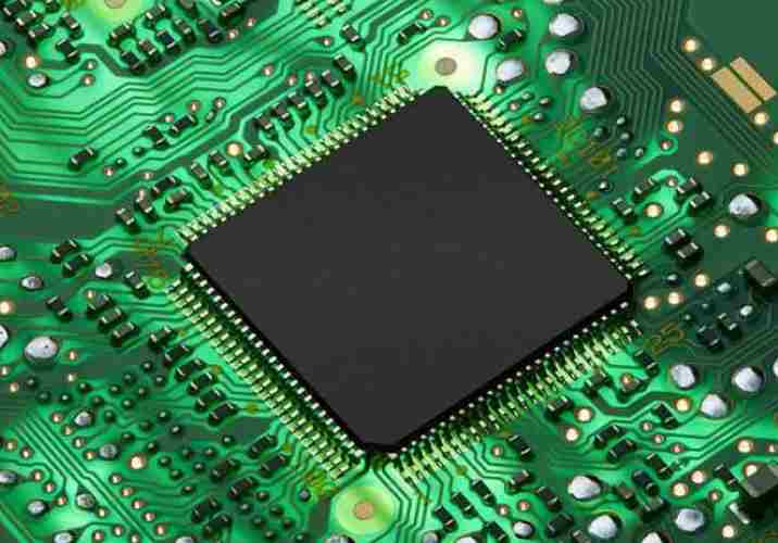
PCB copy board, the industry is also often referred to as board copy board, board clone, board copy, PCB clone, PCB reverse design or PCB reverse research and development.
In other words, on the premise of existing physical electronic products and circuit boards, reverse analysis of circuit boards is carried out by using reverse R&D technology means, and the original product's PCB file, bill of materials (BOM) file, schematic file and other technical documents as well as PCB silkscreen production files are 1:1 restoration. Then use these technical documents and production documents to make PCB board, component welding, fly needle testing, circuit board debugging, and complete the complete copy of the original circuit board template.

For PCB copy board, many people do not understand, in the end what is PCB copy board, some people even think PCB copy board is copycat. But PCB copying board is definitely not imitating. The purpose of PCB copying board is to learn the latest foreign electronic circuit design technology, and then absorb the excellent design scheme, and then used to develop and design more excellent products.
With the continuous development and deepening of the board copying industry, today's PCB board copying concept has been extended to a wider range, is no longer limited to simple circuit board copying and cloning, but also involves the secondary development of products and the research and development of new products.
For example, through the analysis of existing product technical documents, the understanding and discussion of design ideas, structural features and process technology, it can provide feasibility analysis and competitive reference for the research and development design of new products, assist research and development design units to timely follow up the latest technological development trend, timely adjust and improve product design schemes, and develop the most competitive new products in the market.
Through the extraction and partial modification of the technical data files, the process of PCB board copying can realize the rapid update and upgrade of various types of electronic products and secondary development. According to the document drawing and schematic diagram extracted from the board copying, professional designers can also optimize the design and change the PCB board according to the wishes of customers. On this basis, new functions can be added to the product or functional features can be redesigned. In this way, the product with new functions will appear in the fastest speed and new attitude. It not only owns its own intellectual property rights, but also wins the opportunity in the market, bringing double benefits to customers.
Whether it is used to analyze circuit board principles and product performance in reverse research, or reused as the basis and basis of PCB design in forward design, PCB schematics have a special role.
Then, according to the document diagram or the real thing, how to carry out the PCB schematic backsliding, the backsliding process is what? What details should I pay attention to?
Backward step
01
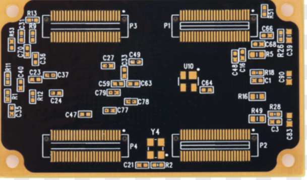
Record PCB details
Get a PCB, first of all on the paper record the model, parameters, and position of all components, especially the diode, the direction of the three-stage tube, the direction of the IC notch. It's best to take two pictures of the device's location with a digital camera. A lot of pcb circuit boards do more advanced above the diode transistor some do not pay attention to see.
02
Scanned image
Remove all the components and remove the tin from the PAD hole. The PCB is cleaned with alcohol and placed in a scanner, which scans with slightly higher pixels to get a sharper image. Then the top and bottom layers are lightly polished with gauze paper until the copper film shines, put them in the scanner, start PHOTOSHOP, and sweep the two layers in color separately.
Note that PCB must be placed horizontally and vertically in the scanner, otherwise the scanned image cannot be used.
03
Adjust and correct image
Adjust the contrast and brightness of the canvas so that the part with copper film is in strong contrast with the part without copper film, then turn the subdrawing to black and white, check whether the lines are clear, if not, repeat this step. If it is clear, save the picture as black and white BMP format files TOP BMP and BOT BMP. If there is any problem with the picture, you can use PHOTOSHOP to repair and correct it.
04
Verify the position coincidence between PAD and VIA
The two BMP files are converted into PROTEL files respectively, and two layers are transferred into PROTEL. If the positions of PAD and VIA after two layers are basically identical, it indicates that the previous steps have been done well. If there is any deviation, repeat the third step. So pcb copying board is a very patient work, because a little problem will affect the quality and the degree of matching after copying board.
05
Drawing layer
Convert the BMP of the TOP layer to the TOP PCB, be careful to convert to the SILK layer, which is the yellow layer. Then you trace the line on the TOP layer and place the device according to the drawing of step 2. Delete the SILK layer when you are done. Repeat until all layers are drawn.
06
Record PCB details
TOP PCB and BOT PCB are combined
07
Laser printing TOP LAYER, BOTTOM LAYER
Use a laser printer to print the TOP LAYER and BOTTOM LAYER onto the transparent film (1:1 ratio), place the film on the PCB, compare and see if it's wrong, if it's right, you're done.
08
Test copy board electronic technology performance is the same as the original board. If it's one, it's really done.
Five requirements for PCB processing
Feb 03,2023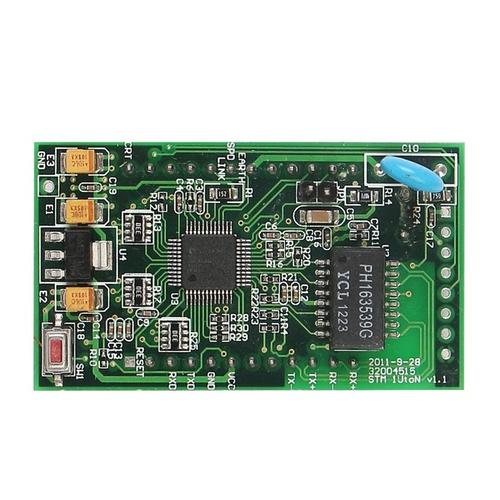


Just upload Gerber files, BOM files and design files, and the KINGFORD team will provide a complete quotation within 24h.