
Professional PCB manufacturing and assembly
Building 6, Zone 3, Yuekang Road,Bao'an District, Shenzhen, China
+86-13410863085Mon.-Sat.08:00-20:00

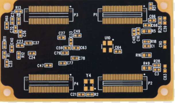
Get a PCB, first of all on the paper record the model, parameters, and position of all components, especially the diode, the direction of the three-stage tube, the direction of the IC notch. It's best to take two pictures of the device's location with a digital camera. A lot of pcb circuit boards do more advanced above the diode transistor some do not pay attention to see.
02
Scanned image
Remove all the components and remove the tin from the PAD hole. The PCB is cleaned with alcohol and placed in a scanner, which scans with slightly higher pixels to get a sharper image. Then the top and bottom layers are lightly polished with gauze paper until the copper film shines, put them in the scanner, start PHOTOSHOP, and sweep the two layers in color separately.
Note that PCB must be placed horizontally and vertically in the scanner, otherwise the scanned image cannot be used.
03
Adjust and correct image
Adjust the contrast and brightness of the canvas so that the part with copper film is in strong contrast with the part without copper film, then turn the subdrawing to black and white, check whether the lines are clear, if not, repeat this step. If it is clear, save the picture as black and white BMP format files TOP BMP and BOT BMP. If there is any problem with the picture, you can use PHOTOSHOP to repair and correct it.
04
Verify the position coincidence between PAD and VIA
The two BMP files are converted into PROTEL files respectively, and two layers are transferred into PROTEL. If the positions of PAD and VIA after two layers are basically identical, it indicates that the previous steps have been done well. If there is any deviation, repeat the third step. So pcb copying board is a very patient work, because a little problem will affect the quality and the degree of matching after copying board.
05
Drawing layer
Convert the BMP of the TOP layer to the TOP PCB, be careful to convert to the SILK layer, which is the yellow layer. Then you trace the line on the TOP layer and place the device according to the drawing of step 2. Delete the SILK layer when you are done. Repeat until all layers are drawn.
06
TOP PCB and BOT PCB are combined
07
Laser printing TOP LAYER, BOTTOM LAYER
Use a laser printer to print the TOP LAYER and BOTTOM LAYER onto the transparent film (1:1 ratio), place the film on the PCB, compare and see if it's wrong, if it's right, you're done.
Reasonable division of functional areas
In the reverse design of a good PCB circuit board schematic, reasonable division of functional areas can help engineers reduce some unnecessary trouble and improve the efficiency of drawing.
Generally speaking, the components with the same function on a PCB board will be centrally arranged, and the functional division of the area can be a convenient and accurate basis for the backdrawing of the schematic. However, the division of this functional area is not arbitrary. It requires engineers to have some knowledge of electronic circuits.

First, find out the core components in a certain functional unit, and then find out other components of the same functional unit according to the wiring connection, and form a functional partition (the formation of functional partition is the basis of schematic drawing). Also, during this process, don't forget to use the component numbers on the circuit board, which can help you partition functions faster.
02
Find the right benchmark
This reference piece can also be said to be the main component PCB network city at the beginning of schematic drawing. After determining the reference piece, drawing according to the pins of these reference pieces can ensure the accuracy of schematic diagram to a greater extent.
For engineers, the determination of the reference is not a very complex thing, in general, you can choose to play a major role in the circuit components as the reference, they are generally larger, more pins, easy to draw, such as integrated circuit, transformer, transistor and so on, can be used as a suitable reference.
03
Correctly distinguish lines and reasonably draw wiring
For the distinction of ground wire, power cord and signal line, engineers also need to have relevant knowledge of power supply, circuit connection knowledge, PCB wiring knowledge and so on. The distinction of these lines can be analyzed from the connection of components, the width of copper foil and the characteristics of the electronic products themselves.
In wiring drawing, in order to avoid crossing and interspersing lines, a large number of ground symbols can be used for ground wires. Different lines of different colors can be used to ensure clear identification. Special marks can also be used for various components, and unit circuits can even be drawn separately and then combined.
04
Master the basic framework, learn from similar schematic diagram
For some basic electronic circuit framework and schematic method, engineers need to master, not only to be able to draw some simple and classic basic cell circuit composition form directly, but also to form the overall framework of electronic circuit.
On the other hand, do not ignore that the schematic diagram of the same type of electronic products has certain similarities to PCB network city, engineers can fully draw lessons from the similar circuit diagram according to the accumulation of experience to carry out the new product schematic backsliding.
05
Check and optimization
After the schematic drawing is completed, the reverse design of PCB schematic diagram can be concluded only after testing and checking. The nominal values of components sensitive to PCB distribution parameters need to be checked and optimized. The schematic diagram is compared, analyzed and checked according to the PCB file diagram to ensure that the schematic diagram is completely consistent with the file diagram.


Just upload Gerber files, BOM files and design files, and the KINGFORD team will provide a complete quotation within 24h.