
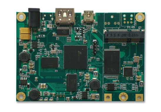
Professional PCB manufacturing and assembly
Building 6, Zone 3, Yuekang Road,Bao'an District, Shenzhen, China
+86-13410863085Mon.-Sat.08:00-20:00

Many people think that the price is not very cheap for SMT proofing small batch processing, and I believe that many customers will have such a feeling. It is clear that I only do ten and twenty pieces of SMT processing, why do I charge more than 1000 processing fee? The price is a little black.
Many customers who have just come into contact with SMT patch processing industry should have such an experience. Originally, they went to the processing plant with the mentality that they could get it done with three or five hundred. As soon as the offer came in, it was several times over budget. When they see the price, they will go directly to find an SMT factory for quotation, and the result is usually similar. Next, kingford, Shenzhen SMT processing manufacturer, will introduce the reasons for the high price of small batch processing of SMT proofing.
SMT proofing small batch processing price is high
Small batch patch proofing costs mainly include start-up fees, engineering fees, steel mesh fees, processing fees calculated according to conventional points, or summarized directly with the minimum consumption. The minimum consumption is actually the capital protection cost of the electronics processing plant. If this cost is insufficient, you are likely to make no money or even lose money. No one runs a losing business.
The normal batch of SMT patch proofing processing is generally calculated directly according to the point cost plus steel mesh fee, the point calculation standard is generally 0.002-0.03 yuan/point is normal, if there are special requirements, it may be a little more expensive. SMT patch proofing in small batches is expensive because there are not so many necessary costs to be shared in the process. In the actual processing, there is no big difference between 1 board and 100 boards of pure patch, which is finished in a short time, but the processing process is the same, such as component detection, sample storage system, tin paste temperature mixing, PCB baking, patch programming, SPI detection, AOI detection, first piece detection, aging test, assembly, packaging and shipping and other processing processes are necessary. The above cost of labor is actually the same, but that large quantities have so much to carry out cost allocation, small batch can not be allocated, this is the reason for charging start-up fees or engineering fees.
In addition to the incompresable labor cost, the production efficiency will also be seriously reduced. SMT sample making in small batches will stop when the production line is just started, which undoubtedly has a great impact on the production efficiency. Generally speaking, the low price proofing single is configured with a special proofing production line or a small workshop manual patch.

2. Why can't signal lines be changed multiple times in high-speed PCB design?
Why can't the signal line be changed multiple times in high speed PCB design? Everyone must have touched the hole in PCB design, so we all know that the hole has a great impact on the quality of PCB signal. First, let us introduce how to select the hole in PCB design.
There are usually three types of perforations to choose from: (in mil)
8/16±2mil 10/20±2mil 12/24±2mil
Usually, when the board is relatively dense, we will use the size of 8/16±2mil(8/14,8/16,8/18) hole, when the board is relatively open, you can choose the size of 12/24±2mil(12/22,12/24,12/26 all right) hole, A pass hole of 10/20±2mil(10/18,10/20,10/22) size can be used between 10/20.
In terms of economic benefits, the bigger the hole, the lower the cost, so we want to control the cost of the plate, in order to meet our design at the same time, as far as possible to set the hole a little larger.
Of course, in HDI boards, we usually need blind burials. Usually, the size of our blind hole ranges from 4/10±2 so that it can usually hit the pad, but it should be noted that it should not hit the center of the pad. It can usually hit the edge of the pad, which is better in terms of processing.
So do we have a bigger hole or a smaller hole, which is obviously not the case.
From the point of view of the process, our hole diameter should not be less than 1/7 of the plate thickness, why?
Because when our through hole is less than 1/7, due to the influence of the process technology, we can not uniformly plated copper on the through hole wall, when we can not uniformly plated copper, the electrical performance of our plate will be affected. Therefore, when the plate thickness is larger, we should also increase the hole.
Our conclusion above is that it's better to go through a bigger hole. At this point, we need to introduce you to two formulas. One is the formula for calculating the parasitic capacitance through the hole: C= 1.4ε TD2/ (D1-D). The other is the formula for calculating the parasitic inductance: L=5.08h[ln (4h/d) +1].
First look at the calculation formula of pore parasitic capacitance:
ε : The dielectric constant of the plate. The dielectric constant varies from plate to plate. T: the thickness of the fingerboard.
Suppose the through-hole is in GND. In this case, D1 is the avoiding distance between the through-hole edge and the copper skin (back pad). D2: refers to the outside diameter of the through-hole.
We can draw a conclusion from the above formula:
1. When the plate and plate thickness remain unchanged, the larger the parasitic capacitance of D, the smaller the parasitic capacitance, and the inversely proportional relationship between C and D1.
2. When the plate and thickness remain unchanged, the larger the parasitic capacitance of D is, the larger the parasitic capacitance is, and C is proportional to D2.
3. When the plate thickness and D2 and D are unchanged, the larger the dielectric constant of the plate, the larger the parasitic capacitance, and the C is proportional to the ε.
4. The larger the dielectric constant and D2, the larger the parasitic capacitance.
In common PCB design, parasitic capacitance and inductance through holes have little influence on PCB design, which can be used as a conventional choice. But at high speed. Through the analysis of the above parasitical characteristics of PCB, we can see that the intermediate perforation design at high speed in the design of PCB, seemingly simple perforation will often bring huge negative impact on circuit design.
In order to reduce the adverse effects of the parasitic effect of pores, the design can be as far as possible:
1) Select a reasonable hole size. For multi-layer general density PCB in the design, choose 10/20/36POWER isolation zone) through the hole is better; For the power supply or ground wire hole, may consider using a larger size, in order to reduce impedance;
2) The bigger the POWER quarantine zone, the better;
3) PCB signal routing should not change layers as far as possible, that is, to reduce holes as far as possible;
4) The use of thinner PCB two parasitic parameters is conducive to reducing holes;
Of course, specific problems need to be analyzed in the design. Considering cost and signal quality, at high speed PCB design, designers always want the hole as small as possible, the more wiring space on the template. In addition, the smaller the hole, the smaller its own parasitic capacitance, more suitable for high-speed circuits.
In the design of high density PCB, the decrease of non-pass hole (blind hole) and pass hole size brings the increase of cost. The pass hole size can not be reduced indefinitely, which is affected by the PCB manufacturer at high speed limit drilling and electroplating and other technology PCB should consider balance in the design of through hole.
Then, after understanding the above information, we will know why we should not punch too many holes in high speed PCB design. The hole itself will introduce parasitic capacitance and parasitic inductance. The more holes, the larger the value of the parasitic capacitance and the parasitic inductance. So this is why a lot of data manuals will write that the number of holes when we wire can not exceed how many, generally our high-speed signal line can not take more than three holes, can not punch the hole.


Just upload Gerber files, BOM files and design files, and the KINGFORD team will provide a complete quotation within 24h.