
Professional PCB manufacturing and assembly
Building 6, Zone 3, Yuekang Road,Bao'an District, Shenzhen, China
+86-13410863085Mon.-Sat.08:00-20:00

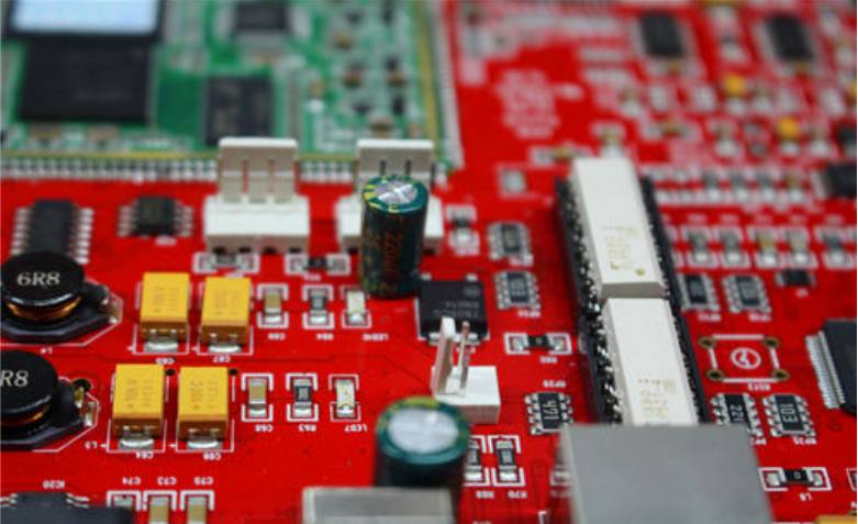
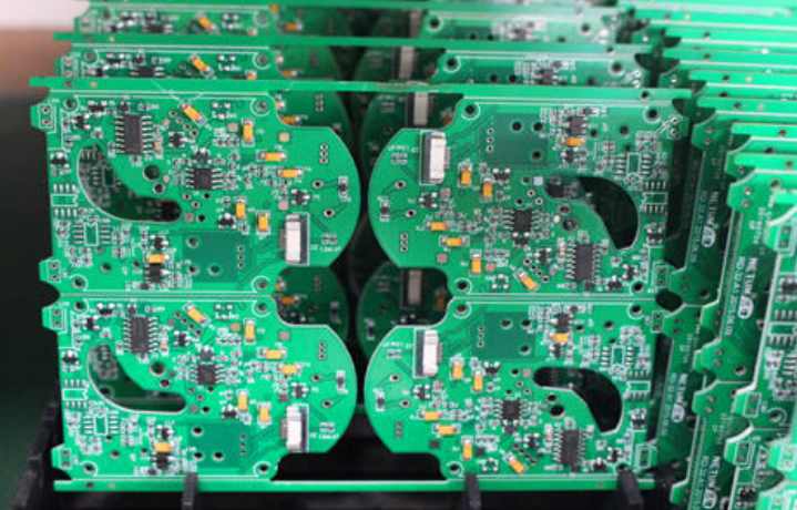
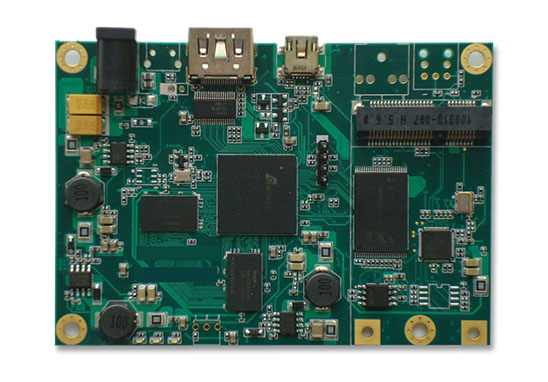
Circuit board is the necessary material of PCBA processing plant, circuit board is mainly to provide a carrier for various electronic components, and components link together to form a complete circuit. The manufacture of the circuit board is more complex, next to understand some basic knowledge of the circuit board process.
1. Printed circuits provide the following functions in electronic equipment:
1. Provide mechanical support for fixing and assembling various electronic components such as integrated circuits.
2. Realize wiring and electrical connection or electrical insulation between various electronic components such as integrated circuits.
3, provide the required electrical characteristics, such as characteristic impedance, etc.
4. Provide solder resistance graphics for automatic soldering, and provide identification characters and graphics for component insertion, inspection and maintenance.
Two, some basic terms about printed board
On the insulating substrate, according to the predetermined design, made of printed circuit, printed element or a combination of the conductive graphics, known as printed circuit. On the insulating substrate, a conductive pattern of electrical connection between elements and devices is provided, which is called printed circuit. It does not include printed components. Printed circuit of the finished board called printed circuit board, also known as printed board. Printed boards can be divided into two categories according to whether the substrate used is rigid or flexible: rigid printed boards and flexible printed boards. This year has seen the emergence of rigid ----- flexible combination of printed boards. According to the conductor graphic layer number can be divided into single - sided, double - sided and multilayer printed board. A printed board in which the entire outer surface of the conductor pattern is in the same plane as the surface of the substrate is called a flat board.
For terms and definitions of printed circuit boards, see National Standard GB/T2036-94 "Printed Circuit Terminology".
Electronic equipment using printed board, because of the consistency of similar printed board, so as to avoid the error of manual wiring, and can realize the automatic insertion or installation of electronic components, automatic soldering, automatic detection, to ensure the quality of electronic equipment, improve labor productivity, reduce costs, and easy maintenance.
Printed boards evolved from single-layer to double-sided, multilayer and flexible, and continue to evolve separately. Due to the continuous development to the direction of high precision, high density and high reliability, and constantly reduce the size, reduce the cost, improve the performance, so that printed board in the future development of electronic equipment engineering, still maintain strong vitality.
Three. Signs of the technical level of printed boards:
For double-sided and multi-hole metallized printed boards, the number of wires that can be laid between two pads at the intersection of the 2.50 or 2.54mm standard grid is a mark of the number of double-sided metallized printed boards that are mass-produced
A wire is arranged between two pads and is a low density printed board with a wire width greater than 0.3mm. The medium density printed board is provided with two wires arranged between the two pads, and the width of the wires is about 0.2mm. Three wires are arranged between two pads, which is a high-density printed board with a wire width of about 0.1-0.15mm. Four wires are arranged between the two pads, and the ultra-high density printed board can be calculated, with a wire width of 0.05-0.08mm.
A foreign magazine has introduced the printed board which can be arranged with five wires between two pads.
For the multilayer board, should also be aperture size, the number of layers as a comprehensive measure mark.
Development trend of PCB advanced manufacturing technology
The development trend of printed board manufacturing technology is basically the same at home and abroad, that is, to high density, high precision, fine aperture, fine wire, fine spacing, high reliability, multi-layer, high-speed transmission, light weight, thin shape, in production at the same time to improve productivity, reduce cost, reduce pollution, adapt to the direction of multi-variety, small batch production. The level of technical development of printed circuits is generally represented by line width, aperture and plate thickness/aperture ratio on printed boards.
Four, PCB manufacturing process
1. Film base version
The quality of film substrate directly affects the quality of printed board production. When producing a printed circuit board, there must be at least one set of corresponding film substrates. There should be at least one film negative for each conductive pattern (signal layer circuit pattern and ground, power layer pattern) and non-conductive pattern (solder resistance pattern and character) of the printed board. Through the photochemical transfer process, all kinds of graphics are transferred to the production plate.
The uses of film substrate in printed board production are as follows:
(1) Photomask graphics in graphics transfer, including circuit graphics and photoresist welding graphics.
(2) The production of screen templates in the screen printing process, including solder resistance graphics and characters.
(3) Machining (drilling and profile milling) CNC machine tool programming basis and drilling reference.
With the development of electronic industry, the demand for printed board is becoming higher and higher. Printed board design of high density, fine wire, small aperture trend faster and faster, printed board production process is becoming more and more perfect. In this case, it is difficult to produce high-quality printed circuit boards without high-quality film underprints. Modern printed board production requires the following conditions to be met:
The dimensional accuracy of the film substrate must be the same as that required for the printed board, and the deviation caused by the production process should be compensated.
The graphics of the film base should meet the design requirements and the graphic symbols should be complete.
The graphic edge of the film version is straight and neat, and the edge is not false; Black and white contrast to meet the requirements of photosensitive process.
The film substrate material should have good dimensional stability, that is, small dimensional changes due to changes in ambient temperature and humidity.
Double panel and multilayer film base plate, the welding pad and common graphics required good coincidence accuracy.
The layers of the Fillings should be clearly marked or named.
Film substrate can pass through the required wavelength of light wave, the general sensitive wavelength range is 3000- 4000A.
In the past, it was generally necessary to make a photographic base, and then to complete the production of the film base. In recent years, with the rapid development of computer technology, the production process of the film version has also developed greatly. Using advanced laser light drawing technology, greatly improve the production speed and the quality of the base plate, and can produce high precision, fine wire graphics that can not be completed in the past, so that the CAM technology of printed board production tends to be perfect
2. Substrate material
Copper clad laminates (CopperCladLaminates, abbreviated as CCL), the copperclad foil or copperclad sheinates and serves as the base plate material of PCB. At present, the most widely used etching method of PCB circuit board, is the selective etching on the coppered foil board, to obtain the required line pattern. Copper clad board in the whole printed circuit board, mainly responsible for the conduction, insulation and support of three aspects of the function. The performance, quality and manufacturing cost of printed boards depend largely on copper-covered foil boards.
In the process of larger electronic product research, the most fundamental success factor is the design, documentation and manufacture of the printed board for that product. The design and manufacturing quality of printed board directly affect the quality and cost of the whole product, and even lead to the success or failure of commercial competition.


Just upload Gerber files, BOM files and design files, and the KINGFORD team will provide a complete quotation within 24h.