
Professional PCB manufacturing and assembly
Building 6, Zone 3, Yuekang Road,Bao'an District, Shenzhen, China
+86-13410863085Mon.-Sat.08:00-20:00

Research and Suggestions on Surface Treatment Technology of Lead free PCB
The emergence of lead-free technology PCB board has raised new problems for in circuit testing (ICT) This paper describes the existing PCB surface treatment processes, and analyzes the impact of these processes on ICT It was pointed out that the key to ICT is the probe and ICT The contact reliability between points is tested, and the specific changes needed in PCB construction are described to meet ICT requirements Historically, the main focus of a test engineer is to ensure that he has an effective test program that performs well in production "In-Circuit Test (ICT)" remains a very effective method of detecting manufacturing defects. More advanced ICT systems can also add real value to test functions by providing flash memory programming methods, such as PLD, FPGA, and EEPROM during testing Agilent 3070 system can be sold in ICT ICT still plays an important role in the manufacturing and testing process of the printed circuit board assembly (PCA)? The promotion of lead-free soldering technology has led to a lot of research on surface treatment technology These studies are mainly based on the technical performance during PCB construction The influence of different PCB surface treatment technologies on the test stage is mostly ignored, or only the contact resistance is concerned This book will describe in detail the impacts observed in ICT and the need to respond to and understand these changes
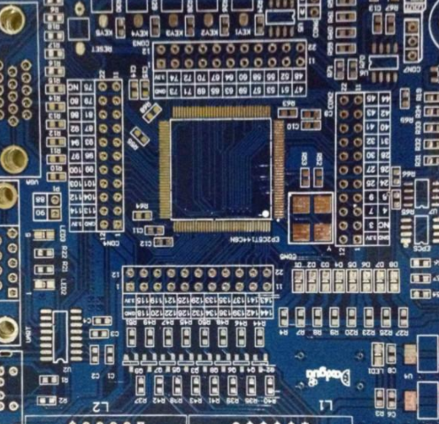
PCB board

The purpose of this paper is to share the following experience: PCB surface treatment and training engineers to implement changes in ICT PCB production process requirements This paper will discuss the surface treatment of lead-free PCB, especially in the ICT stage of the manufacturing process, and reveal that the successful test of lead-free surface also depends on the beneficial contribution of PCB construction process A successful ICT test is always based on the physical characteristics of the contact point between the test probe of the needle bed fixture and the test pad on the PCB When a very sharp probe contacts a weld test point, the solder will sink because the contact pressure of the probe is much higher than the yield strength of the solder Because the solder is recessed, the probe passes through any impurities on the surface of the test pad The following uncontaminated solder now contacts the probe and is in good contact with the test point The probe insertion depth is a direct function of the yield strength of the target data The deeper the probe penetrates, the better the contact An 8-ounce (oz) probe can apply contact pressures ranging from 26,000 to 160,000 pounds per square inch, depending on the surface diameter Because the yield strength of solder is about 5000 psi, the probe contact is better for this relatively soft solder
1. Selection of PCB surface treatment process
Before we understand causality, it is important to describe the types of PCB surface treatments available and what they can provide. All printed circuit boards (PCBs) have copper layers. If they are not protected, the copper layers will be oxidized and damaged. A variety of different protective layers can be used, including hot air solder leveling (HASL), organic solder protection (OSP), electroless nickel gold immersion (ENIG), silver immersion and tin immersion.
2. Hot air solder leveling (HASL)
HASL is the main lead containing surface treatment process used in industry. The process is formed by immersing the circuit board into the lead tin alloy, and the excess solder is removed by "air knife", which is hot air blown on the surface of the circuit board. For PCA process, HASL has many advantages: it is a PCB board, and the surface layer can be welded after repeated reflow, cleaning and storage. For ICT, HASL also provides automatic solder coverage for test pads and through holes. However, the flatness or coplanarity of HASL surface is poor compared with the existing alternative methods. There are some lead-free HASL replacement processes. Due to the natural replacement characteristics of HASL, these processes are becoming more and more popular. Over the years, HASL has been used effectively, but with the emergence of "environmental protection" green process requirements, the days of this process are numbered. In addition to the lead-free problem, the new complexity of the board and the finer spacing exposed many limitations of the HASL process. Advantages: Low cost PCB surface technology keeps solderability throughout the manufacturing process and has no negative impact on ICT. Disadvantages: Usually lead based process is used, but it is currently limited and will be eliminated in 2007. For thin pin spacing (<0.64mm), solder bridging and thickness problems may occur. The non-uniformity of the surface will lead to the uniformity problem in the assembly process.
3. Organic solder protector
Organic solder preservative (OSP) is used to form a thin and uniform protective layer on the copper surface of PCB. This coating protects the circuit from oxidation during storage and assembly operations. This process has been around for a long time, but it has only recently become popular with the search for lead-free technology and fine pitch solutions. In terms of coplanarity and solderability, OSP is superior to HASL in PCA assembly, but it requires significant process changes to the type of flux and the number of hot cycles. Care should be taken as its acidity will reduce OSP efficiency and make copper easy to oxidize. Assemblers prefer to use metal surfaces that are more flexible and can withstand more cycles of thermal cycling. For OSP surface treatment, if the test point is not welded, it will lead to the contact problem of ICT needle bed fixture. Simply changing to a sharper probe type to pass through the OSP layer will only cause damage and puncture the PCA test via or test pad. The research shows that switching to higher detection force or changing the probe type has little effect on the output. The yield strength of untreated copper is one order of magnitude higher than that of lead solder, which will damage the exposed copper test pad. All testability guidelines strongly recommend against direct detection of exposed copper. When using OSP, you need to define a set of OSP rules for the ICT phase. Important rules require that the template be opened at the beginning of the PCB process to allow the solder paste to be applied to the test pads and through holes that ICT needs to contact. Advantages: The organizational cost is equivalent to HASL, coplanarity is good, lead-free process, and solderability is improved. Disadvantages: The assembly process needs significant changes. Detecting the rough copper surface will be harmful to ICT. Over sharp ICT probes may damage PCBs. Manual precautions are required to limit ICT testing and reduce test repeatability.
4. Immersion of electroless nickel plated gold
Electroless nickel gold immersion (ENIG) is a kind of coating successfully applied to many circuit boards. Although its organizational cost is high, its surface is flat and has excellent solderability. The main disadvantage is that the electroless nickel coating is fragile and has been found to crack under mechanical stress. This is called "black block" or "mud crack" in the industry, which has led to some negative reports of Eni Group. Advantages: good weldability, smooth surface, long shelf life, and can withstand repeated reflow welding. Disadvantages: high cost (about 5 times of HASL), "black block" problem, cyanide and other harmful chemicals are used in the manufacturing process.
5. Silver immersion
Silver dipping is an additional method of PCB surface treatment. It is mainly used in Asia and is being promoted in North America and Europe. During welding, the silver layer melts into the solder joint, leaving tin/lead/silver alloy on the copper layer, providing a very reliable solder joint for BGA packaging. Its contrast color makes it easy to check, and it is also a natural substitute for HASL welding treatment. Silver plating is a very promising surface treatment process, but like all new surface treatment technologies, the end user is very conservative about it. Many manufacturers refer to this process as "under investigation", but it may be the preferred lead-free surface process. Advantages: good weldability, smooth surface, can replace HASL immersion. Disadvantages: The conservative attitude of end users means that the industry lacks relevant information.
6. Tin dipping
This is a relatively new surface treatment process, which has many similar effects to silver immersion process. However, due to the preventive measures of using thiourea (possibly carcinogen) during tin impregnation in PCB manufacturing, there are significant health and safety problems. In addition, migration ("tin burr" effect) also deserves attention, although anti migration chemistry can achieve some success in controlling this problem. Advantages: good weldability, smooth surface and relatively low cost. Disadvantages: health and safety issues, limited number of hot cycles.
7. Summary of PCB surface treatment
Considering some problems of fixture and process, users believe that once these problems are solved, they can obtain 80~90% qualification rate. These are the main methods for lead-free processing of PCB. HASL will still be a widely used PCB processing process. In this case, the test engineer will not change anything. In some countries, HASL has been prohibited by law and has adopted alternative solutions. As PCA manufacturing expands to more different fields, more and more lead-free processes will appear in ICT testing. Although OSP is not a natural substitute for HASL, it has become an alternative treatment scheme being studied by PCA manufacturers. When no process change is made to allow the use of solder paste on test pads and vias, this will result in actual ICT
Test reliability problems
The conclusion is that the process of PCB surface treatment is not perfect, and each method has its own problems to consider. Some of these problems are more serious than others. All these lead-free PCB surface preparation processes need to be modified in the process steps to prevent ICT fixture contact reliability problems. Comparison of HASL, OSP and silver plating in ICT stage Now I want to focus on these surface treatment technologies and their impact on ICT efficiency. The surface treatment leaves soft soldering "arc" and exposed through-hole at the test point, which is an ideal choice for ICT test objects. The characteristic of HASL that OSP does not have is force absorption. HASL is an eutectic SnPB, which is particularly soft. This soft target has two advantages: adapting to the probe and absorbing energy. The OSP PCB has no such soft target. In contrast, the copper surface is very hard and cannot absorb so much energy. The direct contact area that this probe can "bite" into is reduced. The copper coating on the outer layer is usually between 10 microns and 50 microns. Combine the copper plating with the OSP coating, and you will see that the probe used to detect the HASL board will not work on the OSP veneer. The research shows that OSP forms a very hard "shell" on the test target in a long transmission time between reflow soldering and ICT. ICT delivery time should be less than 24 hours. There are many other process factors that can affect the degree of confusion that OSP has with test engineers, some of which include the type of OSP supplier, the number of passes in the reflow furnace, whether the wave process has been removed, nitrogen or air reflow, and the type of ICT analogy testing. The direct detection of the copper surface combined with the higher detection power required to penetrate the OSP layer creates a real potential threat of damaging the thin copper layer and causing internal short circuits. In this regard, we recommend not to detect exposed copper surfaces. Recent examples have shown that after 5 to 10 clamp excitations, the plate through hole or test point can be pierced. For some PCA manufacturers, the impact of OSP on ICT is so great that they are completely divorced from OSP. Other manufacturers are also learning how to follow the "OSP Rules" listed below. "OSP rules" of ICT test fixtures and programs: have a great impact on the passing rate (FPY); It may be necessary to change the clamp probe to obtain higher force, for example, from 2N to 3N; It may be necessary to change the fixture probe type to a more sharp type; It may be necessary to "press twice" the gripper excitation method, or use pneumatic or mechanical hands; Simulation test program constraints may need to be compromised, open, or even ignored; The research shows that these asterisk rules have relatively little influence on the yield, and the method to ensure reliable test contact is to ensure the welding of test pads. Some manufacturers see OSP as an immediate cost saving alternative to lead-free processes. However, some companies have recently made radical changes and are reviewing their compliance when considering the actual costs associated with production interruptions and delays.

PCB design technology of king ford
Nov 03,2022


Just upload Gerber files, BOM files and design files, and the KINGFORD team will provide a complete quotation within 24h.