
Professional PCB manufacturing and assembly
Building 6, Zone 3, Yuekang Road,Bao'an District, Shenzhen, China
+86-13410863085Mon.-Sat.08:00-20:00


Basic Points of PCB Layout for Switching Power Supply
The conversion of power supply<1 href="1-_href_0" t-rget="_bl-k">PCB layout is an important process, in which this development belongs to power supply products In many cases, a power supply that is perfectly designed on... the paper may not work correctly during the initial debugging due to many problems with this layout belongs to the power supply PCB This basic point belongs to the conversion power supply PCB layout is discussed in detail inside, and some actual PCB layout examples are described In order to adapt to the rapid replacement rhythm of electronic products, product design engineers are more inclined to choose automatic control/DC converter, which is easy to purchase in this market and install multiple sets of DC power supplies directly on this circular board Since the generation of electromagnetic interference will affect the electronic products belonging to this typical activity through this conversion power supply, it becomes very important that the layout of this pair belongs to this power supply to the printed circuit board This layout belongs to the conversion power supplied to the printed circuit board, which is completely different. From..., this layout belongs to the digital circular printed circuit board In the digital circular layout, many digital French fries can be automatically arranged through the P (III) B bo rd software, and the French fries between this connecting line can be automatically connected through the printed circuit board bo rd software This transfer of power to discharge through automatic typesetting will definitely not work correctly Therefore, the planner needs to have a certain understanding that belongs to this basic rule, which belongs to the conversion power supply PCB layout, and this work ethics principle belongs to the conversion power supply
PCB board

1............ The basic points belong to the PCB layout, which belongs to the transfer of power supply
1.1 Capacitor high-frequency filtering characteristics
Electrolytic capacitors usually have large capacitance and large equivalent series inductance. Since its resonant frequency is very low, it can only be used for low-frequency filtering. Tantalum capacitors usually have larger capacitance and smaller equivalent series inductance, and their resonant frequency is higher than that of electrolytic capacitors, which can be used for medium and high frequency filtering. The capacitance and equivalent series inductance of ceramic capacitors are usually very small, and their resonant frequency is much higher than that of electrolytic capacitors and tantalum capacitors, which can be used for high-frequency filtering and bypass circuits. Since the resonant frequency of the small capacitance ceramic capacitor is higher than that of the large capacitance ceramic capacitor, the ceramic capacitor with too high capacitance cannot be selected when selecting the bypass capacitor. In order to improve the high-frequency characteristics of capacitors, multiple capacitors with different characteristics can be used in parallel. Figure 3..... shows the effect of impedance improvement after multiple capacitors with different characteristics are connected in parallel. Basic points of power supply layout 1. The capacitance of the bypass ceramic capacitor should not be too large, and its parasitic series inductance should be as small as possible. Multiple shunt capacitors can improve the high frequency impedance characteristics of capacitors.
1.2........ High frequency filtering characteristics of inductance
In switching power supply, the content provider of inductor shall be controlled as small as possible. At the same time, it must be noted that due to different coil structures, inductors of the same inductance will have different content provider values, and inductions of the same inductance will have different content provider values under two different coil structures. 5..... turns of the inductor are wound in turn. The content provider value of the coil structure is 1/5 of the equivalent parallel capacitance (C) of the turn coil. The 5-turn windings of the inductor are wound in a cross sequence. When windings 4.... And 5 are placed between windings 1, 2 and 3, and windings 1 and 5 are very close, the content provider generated by this coil structure is twice the C value of a turn coil. It can be seen that the content provider values of two inductors with the same inductance are actually several times different. In high-frequency filtering, if the content provider value of the inductor is too large, high-frequency noise will easily be directly coupled to the load through the content provider. This inductor also loses its high-frequency filtering function. On the printed circuit board, V is wired to the load (right) through L in different pipes. In order to reduce the content provider of the inductor, the two pins of the inductor should be as far away as possible. The trace from V inside to the positive pole of RL and V inside to the negative pole of RL should be as close as possible, the parasitic parallel capacitance of inductor should be as small as possible, and the distance between pads of inductor pins should be as far as possible.
1.3 Mirror
The mirror concept in electromagnetic theory will help designers master the PCB layout of switching power supply. The DC current flows through the grounding plane. The return DC current on the formation is now very evenly distributed throughout the formation. High frequency current flowing through the same stratum. At this time, the return AC power on the ground can only flow in the middle of the ground, and there is no current on both sides of the ground. The grounding plane designer should try to avoid placing any power supply or signal trace on the grounding plane. Once the wiring on the ground plane destroys the whole high-frequency circuit, the circuit will generate strong electromagnetic wave radiation, which will damage the normal operation of the surrounding electronic equipment. Avoid placing any power or signal traces on the ground plane.
1.4 High frequency circuit
There are many high-frequency circuits composed of power devices in switching power supply. If the circuit is handled improperly, it will have a significant impact on the normal operation of the power supply. In order to reduce the electromagnetic wave noise generated by the high-frequency loop, the loop area should be controlled very small. High frequency current loop has a large area, which will generate strong electromagnetic interference inside and outside the loop. For the same high-frequency current, when the loop area is very small, the internal and external electromagnetic fields of the loop cancel each other, and the entire circuit will become very quiet. The area of high-frequency circuit shall be as small as possible.
1.5 Through hole and pad placement
Many designers like to place many through holes under multilayer printed circuit boards. However, it is necessary to avoid placing too many paths on the high-frequency current return path. Otherwise, the high-frequency current trace on the ground will be damaged. If some through holes must be placed on the high frequency current path, space can be left between the through holes so that the high frequency current can pass smoothly. The through-hole arrangement should not interfere with the high-frequency current on the grounding plane. The designer should also be aware that different pad shapes will produce different series inductances. The arrangement of bypass capacitor shall also consider its series inductance. The bypass capacitor must be a ceramic capacitor with low impedance and low ESL. However, if a high-quality ceramic capacitor is placed in the wrong pipe on the PCB, its high-frequency filtering function will disappear.
1.6. Power DC output
Many switching power supplies have loads that are far from the power output port. In order to avoid electromagnetic downward interference to the output wiring caused by the power supply itself or surrounding electronic equipment, the output power wiring must be very close to minimize the area of the output current loop.
1.7. Separation of ground plane on system board
The system board of the new generation of electronic products will have analog circuit, digital circuit and switching power circuit at the same time. In order to reduce the influence of switching power supply noise on sensitive analog and digital circuits, it is usually necessary to separate the grounding planes of different circuits. If multilayer PCB is used, the ground plane of different circuits can be separated by different PCB layers. If there is only one ground plane for the whole product, whether it is the ground plane separation on the multi-layer printed circuit board or the ground plane separation on the single-layer printed circuit board, the ground plane of different circuits should be connected to the ground plane of the switching power supply through a single point. The seven different circuits on the system board need different grounding planes, and the grounding planes of different printed circuit boards are connected to the power grounding plane through a single point.
2. Example of switching power supply PCB layout
The designer shall be able to distinguish components in the power circuit and components in the control signal circuit on the circuit diagram. If the designer considers all components in the power supply as components in the digital circuit, the problem is quite serious. In general, it is necessary to know the high-frequency current path of the power supply, and distinguish the small signal control circuit and power circuit components and their tracks. Generally speaking, the power circuit of power supply mainly includes input filter capacitor, output filter capacitor, filter inductor and upper and lower power FET. The control circuit mainly includes PWM control chip, bypass capacitor, bootstrap circuit, reverberation voltage divider and reverberation compensation circuit.
2.1 PCB layout of power circuit
The correct placement and routing of the power supply components on the printed circuit board will determine whether the entire power supply works properly. The designer must first have a certain understanding of the voltage and current waveforms on the switching power supply equipment. Current and voltage waveforms of the step-down switching power supply circuit components. Since the current flows from the input filter capacitor (C inside), the upper field effect transistor ((S1)) and the F end field effect transistor ((S2)) to the alternating current with high frequency and high peak value, the loop area formed by C inside - S1-S2 should be minimized. At the same time, the loop area formed by S2, L and output filter capacitor (C) shall also be minimized. If the designer does not make the power supply PCB according to the points described in this book, the power supply PCB shown in Network 19 may be made. There are many errors in PCB layout: because C has a large ESL in it, the high value frequency filtering ability of C in it basically disappears; Secondly, the area of C inside - S1-S2 and S1L (Kut) loops is too large, and the electromagnetic noise generated will cause great interference to the power supply itself and the surrounding circuits; Third, if the L pad is too close, the content provider will be too large, and its high-frequency filtering function will be reduced; Fourthly, the lead wire of the Kurt pad is too long, which leads to too large FSL and loss of high-frequency filter line. The area of C inside - S1-S2 and S2-L-Kut rings has been controlled. The connection point between the source of S1, the drain of S2 and L is a single copper pad. Since the voltage at this junction is high frequency, S1, S2 and L need to be very close. Although there is no peak high-frequency current on the trace between L and Cout, a wider trace can reduce the loss of DC impedance and improve the efficiency of the power supply. If the cost allows, the power supply can be used on a double-sided PCB with a grounding plane on one side, but care must be taken to avoid power lines and signal lines on the grounding plane. Ceramic capacitors are added to the input and output ports of the power supply to improve the high-frequency filtering efficiency of the power supply.
2.2 PCB layout of power control circuit
The PCB layout of power control circuit is also very important. The unreasonable layout will lead to the drift and oscillation of the output voltage of the power supply. The control circuit should be placed on one side of the power circuit, not in the middle of the high-frequency AC circuit. The bypass capacitor shall be as close as possible to the Vcc and grounding pin ((GND)) of the chip. The reverberation divider is also placed near the chip. The circuit from chip drive to FET should also be as short as possible, and the circuit from control chip to upper and lower FET should be as short as possible.
2.3 Example of switching power supply PCB layout 1
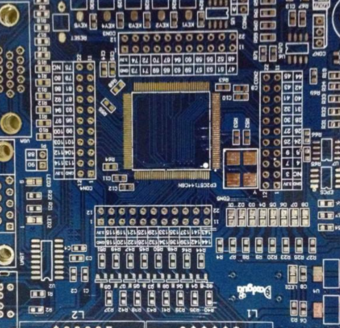
The power supply adopts low-cost PWM controller (Semtech model SCIIO4A.). The lower layer of PCB board is a complete grounding plane. There is no separation between the power plane and the control plane on the PCB. It can be seen that the power circuit of the power supply consists of an input socket (upper left end of the PCB board), an input filter capacitor (C1, (C2),), S1, S2, (L1), and an output filter capacitor (C10, C11, C12, C13) until the output socket (lower right end of the PCB board). SC1104A is located at the lower left end of the PCB. Since the current of the power circuit does not pass through the control circuit on the ground plane, it is unnecessary to separate the ground plane of the control circuit from the ground plane of the power circuit. If the input socket is placed at the lower left end of the PCB board, the power circuit current will directly pass through the control circuit on the ground plane, and the two need to be separated.


Just upload Gerber files, BOM files and design files, and the KINGFORD team will provide a complete quotation within 24h.